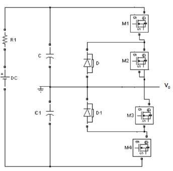
Figure 1. Diode Clamped Three Level Inverter
This paper presents a multilevel inverter with harmonics reduction along with the reduction in number of switches. The reduction in harmonic content in the three-level neutral-point-clamped (NPC), capacitor clamped inverter with inductive load is obtained by simulation. Similarly the reduction in harmonic content in the cascaded multilevel inverter is obtained. The percentage (%) THD is calculated for various levels (3, 7 and 9 level). Finally the percentage (%) THD obtained from various levels is compared. The functionality verification of the multilevel inverter circuit is done using PSPICE and MATLAB. The harmonic reduction is achieved by selecting appropriate switching angles.
The multi level inverter was first introduced in 1975. The three level converters was the first multi level inverter introduced. A multilevel converter is a power electronic system that synthesizes a desired output voltage from several levels of dc voltages as inputs. With an increasing number of dc voltage sources, the converter output voltage waveform approaches a nearly sinusoidal waveform while using a fundamental frequencyswitching scheme. The primary advantage of multi level inverter is their small output voltage, resulting in higher output quality, lower harmonic component, better electro magnetic computability, and lower switching losses[2]. Multilevel inverter include an array of power semiconductors and capacitor voltage sources, the output of which generates voltages with stepped waveforms with less distortion, less switching frequency, higher efficiency, lower voltage devices and better electromagnetic compatibility[4]. The commutation of the switches permits the addition of the capacitor voltages, which reach high voltages at the output, while the power semiconductors must withstand only reduced voltage.
The first practical multilevel topology is the neutral point clamped (NPC) PWM topology introduced by Nabe.et.al, in 1980. For m-level inverter, dc bus voltage is split into 'm' levels by (m-1) series connected bulk capacitors [2]. Here, diodes clamp the switch voltage to half the level of the dc bus voltage, which is an added advantage of this type. Figure 1 illustrates the building block of a phase-leg diode clamped three level inverter.
In this circuit, the dc bus voltage is split into three levels by two series connected bulk capacitors C1 and C2. The middle point of the two capacitors 'n' can be defined as the neutral point. The diodes D1 and D2 clamp the switch voltage to half the level of the dc bus voltage [4].
The diode clamped three level inverter has been simulated using ORCAD PSPICE-software. The switching pulses and simulated output voltage waveform are illustrated in Figures 2(a) and 2(b) respectively.
Figure 1. Diode Clamped Three Level Inverter
This inverter has a similar structure to that of the Diodeclamped; however it can generate the voltage steps with capacitors connected as shown in Figure 3. The problem with this converter is that it requires a large number of capacitors, which translates to a bulky and expensive converter as compared with the diode-clamped inverter. Besides, the number of transistors used is the same with the diode-clamped inverter.
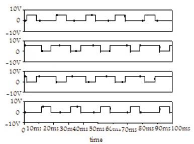
Figure 2(a). Switching Pulses of Three Level Diode Clamped Inverter
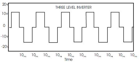
Figure 2(b). Output Voltage of Three Level Diode Clamped Inverter
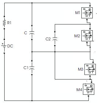
Figure 3. Three Level Capacitor-Clamped Inverter
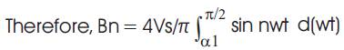
The output voltage of the diode clamped three level inverter is a quarter-wave symmetric stepped voltage waveform. The output voltage will have fundamental and the associated harmonics. These harmonics produce additional heating, when the output voltage of the inverter is fed to the induction motor. The harmonic reduction can be achieved by selecting proper switching angles [1] [6]. The Fourier series of the output is,

Due to half wave symmetry of the output waveform, the even harmonics would be eliminated and possess only the odd harmonics. Hence the average value 'Ao' and constant 'An' are zero[3].
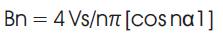
By solving we get,
The third, fifth and seventh harmonics would be eliminated separately if B3 = B5 = B7 = 0, and equation (3) gives the necessary equations to be solved.

Solving these equations, we get corresponding switching angles, therefore third, fifth and seventh harmonics would be eliminated respectively. Table 1 shows the switching pulses of the three level diode clamped inverter calculated using the equation (4).
The performance of three level inverter namely Neutral- Point-Clamped, Capacitor-Clamped inverter with inductive loads are studied. They are individually connected to the inductive loads and their voltage and current waveforms are obtained by simulation. Figure 1 shows the diode clamped inverter connected to an inductive load. The output waveform is shown in Figure 4(a) [6]. The harmonics are analyzed using FFT. The odd harmonics get eliminated as shown in the Figure 4(b).
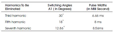
Table 1. Switching Pulse (in milli seconds) for Three Level Diode clamped Inverter
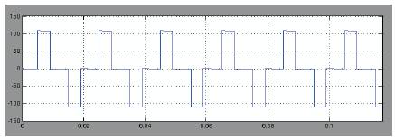
Figure 4a. Output voltage waveform of three level diode clamped Inverter
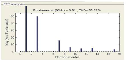
Figure 4b. FFT analysis of three level diode clamped inverter
The Capacitor-Clamped inverter with inductive load is shown in Figure 2. Similarly the output voltage and current waveform with Capacitor-Clamped inverter are studied. The output is shown in the Figures 5(a) and Figure 5(b).
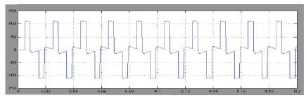
Figure 5a. Output Voltage Waveform of Three Level Capacitor Clamped Inverter
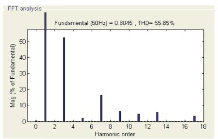
Figure 5b. FFT Analysis of Three Level Capacitor Clamped Inverter
Another characteristic is that the “H” topology has many redundant combinations of switches' positions to produce the same voltage levels. As an example, the level “zero” can be generated with switches in position S(1) and S(2), or S(3) and S(4), or S(5) and S(6), and so on[7] [8] [9]. Another characteristic of “H” converters is that they only produce an odd number of levels, which ensures the existence of the “0V” level at the load .For example, a 51- level inverter using an “H” configuration with transistorclamped topology requires 52 transistors, but only 25 power supplies instead of the 50 required when using a single leg [8]. Therefore, the problem related to increasing the number of levels and reducing the size and complexity has been partially solved, since power supplies have been reduced to 50%.
Figure 6 (a). shows optimized topology of single-phase cascaded inverter. The ac terminal voltages of each bridge are connected in series. Unlike the diode clamp or flying capacitors inverter, the cascaded inverter does not require any voltage-clamping diodes or voltage balancing capacitors. This configuration is useful for constant frequency applications such as active front-end rectifiers, active power filters, and reactive power compensation.
In this case, the power supply could also be voltage regulated dc capacitor. The circuit diagram consists of two cascade bridges. The load id is connected in such a way that the sum of output of these bridges will appear across it. The ratio of the power supplies between the auxiliary bridge and the main bridge is 1:3. One important characteristic of multilevel converters using voltage escalation is that electric power distribution and switching frequency present advantages for the implementation of these topologies[9]. Table 2 shows the switching sequences of the H-bridge inverter to give the stepped output voltage.
Using H-Bridge inverter the harmonics was reduced in 3, 7 and 9 level output voltages. Figure 6(b), 6(c) and 6(d) show the lowest THD level in 3, 7 and 9 level output voltages. The inverter generates a high quality output voltage waveform. It reduces dv/dt stress imposed on power switching devices and also harmonic components of output voltage and load current quite well.
Figure 6a. H- Bridge Inverter
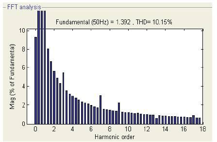
Figure 6b. FFT analysis of H – Bridge 3 Level Inverter
The phase output voltage is synthesized by the sum of two inverter outputs. Each inverter bridge is capable of generating three different levels of voltage outputs. The main bridge can generate +3Vdc, 0, -3Vdc and the auxiliary bridge can generate +Vdc, 0, -Vdc. By using appropriate combinations of switching devices many voltage levels are obtained. When the positive group switches are turned on the voltage across that particular bridge is positive. When the negative group switches are turned on the voltage across that particular bridge is negative. When S1, S2 are turned on the voltage across the main bridge is +3Vdc.
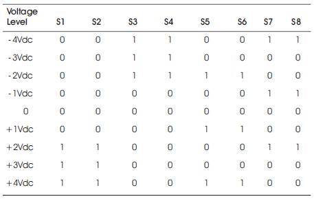
Table 2. Switching Sequence of H – Bridge Inverter
When S3, S4 are turned on the voltage across the main bridge is - 3Vdc.When S5, S6 are turned on the voltage across the auxiliary bridge is +Vdc. When S7, S8 are turned on the voltage across the auxiliary bridge is -Vdc. To obtain +2Vdc the switch combinations S1, S2, S7 & S8 are turned on. To obtain +4Vdc the switch combinations S1, S2, S5 & S6 are turned on. To obtain -2Vdc the switch combinations S3, S4, S5 & S6 are turned on. To obtain -4Vdc the switch combinations S3, S4, S7 & S8 are turned on. Table 3 shows the switching strategy of transistors at each level. The status of the switch is '0', that switch is in OFF condition. The status of the switch is '1', that switch is in ON condition.
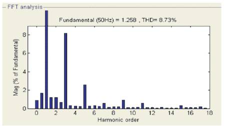
Figure 6c. FFT analysis of H – Bridge 7 Level Inverter
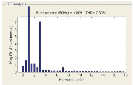
Figure 6d. FFT analysis of H – Bridge 9 Level Inverter
To eliminate 5th, 7th, and 9th order harmonics, the firing angles for each level is found by solving the following equations.
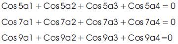
Using Math CAD, the values of “a” is obtained as follows
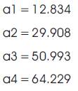
Where,
a1, a2, a3, a4 are the firing angles in degrees.
The output is obtained by carrying out the above calculation. Figure 7 shows the reduction in 7th, 9th and 5th harmonics respectively.
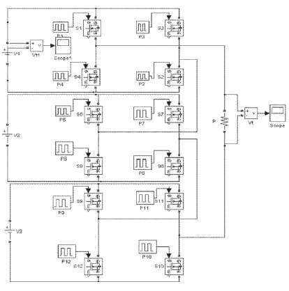
Figure 7. Conventional seven level H- bridge inverter
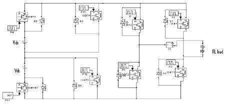
Figure 8. Proposed seven level H-bridge inverter
The H-Bridge 7-level conventional inverter is shown in the Figure 8. The conventional 7- level inverter has some disadvantages as it requires 2(m-1) switching devices; increase the cost; large in size; and controlling is complex.
In order to overcome the above drawbacks the following model has been proposed. The circuit is stimulated in Pspice and the output wave form is obtained. The Figure 8 shows the proposed 7-level inverter. The proposed inverter generates a high quality output voltage waveform. It reduces dv/dt stress imposed on power switching devices. The output waveform shown in the Figures 8(a) and 8(b) show the harmonics represented in THD value.
The THD obtained from various multilevel inverter circuits are compared. The comparison chart is shown. It can be found from Table 4 that with a normal three level capacitor clamped inverter the %THD is 55.85% while that with a diode clamped inverter is 53.27%. But with the use of H-Bridge three level inverter, there is a drastic decrease in the %THD level to 10.15%. Further with the use of HBridge seven level inverter and nine level inverter the %THD are 8.73% and 7.30% respectively. While using the proposed model the %THD level is reduced to 5.79%. This shows an improved performance of the H-bridge inverter.
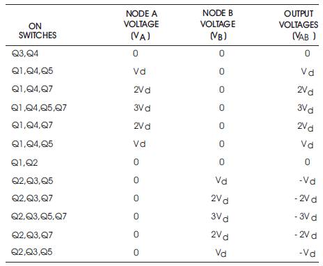
Table 3. Switching Sequence and Output Voltages Levels of Proposed seven level H – bridge Inverter
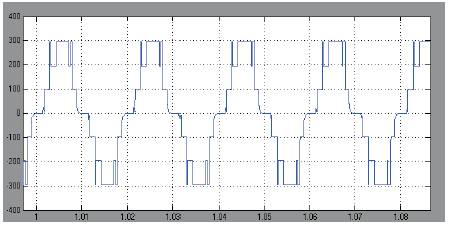
Figure 8a. H – Bridge Proposed Seven Level Inverter Output Voltage
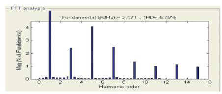
Figure 8b. H – Bridge Proposed Seven Level Inverter FFT Analysis
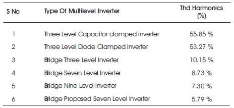
Table 4. Comparison of harmonics in THD Values of various Multilevel Inverters
Performance of multilevel inverter has been presented. Different combinations and topologies were presented. The single phase multilevel inverter has been simulated and harmonics were reduced. Finally the harmonics in multilevel inverter at different stages were compared. From that comparison, it can be seen that the seven level inverter has least value of THD. The simulation results are in line with the prediction.