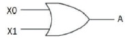
Figure 1. Logic Circuit of 2x1 Encoder
In this paper, Y shaped f2x1 encoder design is based on two dimensional photonic crystals and this encoder design is constructed by point and line defects of photonic crystal which is providing high contrast ratio and reduced power loss for the proposed design. The performances field distributions are analyzed finite difference time domain and the band structures are evaluated using the plane wave expansion method. The proposed 2x1 encoder operated at 1520 nm provides contrast ratio of 28 dB, response time of 3.9 ps, and bit rate of around 0.25 Tbps. So, it is suitable for photonic integrated circuits.
In recent years, high speed communication is required for all optical communications and it provides better performance based on the feature of high speed, high data rate, wide bandwidth compared to electronic devices. Photonic crystal is a periodic material, which is depends on light of the carrier signals for communications. And this photonic crystal is one of the main criteria to design optical devices for the feature of compact size, low loss, and high processing speed. Many optical devices are developed based on photonic crystals. One of main optical devices is encoder. Encoder is designed based on photonic crystal, which is incorporated by many defect mechanisms, such as interference, self-collimated effects, multimode interference, ring resonators, and point and line defects. These mechanisms offer the performance parameters of encoder, such as Contrast ratio, Response time, Transmission efficiency, Delay time, Bit rate, Bandwidth, and Insertion loss.
Many photonic crystal based encoder design is based on logic gates functions. Implementation of photonic crystal based logic gates offer features of increased operating bandwidth, decreasing consumption power, improved response time, and increased contrast ratio for introducing defect mechanisms of interference waveguide, resonator structures, and self collimation phenomenon (Salmanpour, Mohammadnejad, & Bahrami, 2015). The self collimation effect is used to expand the spatial dispersion properties for achieving without diffraction of electromagnetic wave propagation and the determination of effect depends on feature of shape of the photonic crystal dispersion surface (Christina & Kabilan, 2012). The optical logic gates are designed with effects of interference waveguide, where such waveguides, where of structure are coupled to a resonators instead of providing signal propagation in clockwise and counter clockwise direction. Such kind of propagation is delivered partial constructive interference occurrence when the signal is strong and the signal is propagates to the output waveguides (Hussein, Ali, & Rafat, 2018). To implement the design with two coupled heterostructure waveguides, the structure function of interference with constructive and destructive process are coupled to an output waveguide. If the constructive interference is occured in the structure, high power of output signal is delivered and the destructive interference occurrs at the output signal is zero power (Belhadj, Saidani, & Abdelmalek, 2018; Rani, Kalra, & Sinha, 2015).
Multimode Interference effect is another effect for designing all optical logic gates and encoder designs. This method is avoiding signal interference between two waveguides of incident and reflected waves of MMI region in order to achieve high contrast ratio (Haq Shaik, & Rangaswamy, 2017; Saidani, Belhadj, & AbdelMalek, 2015). Another main defect mechanism is line and point defects. Line defects are removing row and column of rods, which is act as waveguide of photonic crystal and the point defect is described by changing structural parameters of rod. This line and point defects based photonic crystal designs are achieving minimum power consumption based devices. The phase difference is applied in two inputs of structure, the constructive and destructive interference signals are obtained which offer logic functions in the proposed designs and the three point defects of the structure is used to control the light signal of logic gates (Goudarzi, Mir, Chaharmahali, & Goudarzi, 2016). Design all optical based OR logic gate with combination of Mach-Zehnder Interferometer (MZI) and line defects, the unwanted power reflection in port to port connection is controlled by implementing Fast Fourier Transform in output port and unexcited input ports. To apply FFT method, the entire structure should be considered as a single cavity (Pirzadi, Mir, & Bodaghi, 2016).
All the optical logic gates and encoder designs have different shapes of waveguides which are connected point and ring resonator, for the purpose of coupling the power signals from input ports into output ports. Such kinds of waveguides are called T-waveguides (Shaik & Rangaswamy, 2018), L-waveguide (Mehdizadeh, Soroosh, & Alipour-Banaei, 2016) and Y-waveguides (Jayabarathan, Subhalakshmi, & Robinson, 2018). The logic gates and 4x2 encoder of low input power based photonic crystal designs have Y shaped line defects, which is coupled to a ring resonators for the reason of permit peak signal from input port to output port (Younis, Areed, & Obayya, 2014; Naghizade & Khoshsima, 2018). Linear and non-linear effects are the main criteria for designing PC based logic gates and encoder designs. Without using non-linear material, the all optical logic NOT gate offers low power and relatively large operating bandwidth (Wu, Liu, & Ouyang, 2012). The non-linear Kerr effects based designs need high input power. So, the all optical 8 to 3 binary encoder design is having linear based structure, which reduces the requirement of high input power (Naghizade, Mohammadi, & Khoshsima, 2018).
PC based ring resonator is another defect in photonic crystal design. Ring resonator is coupled to waveguides for signal propagation in any photonic crystal based optical devices with factor of power loss form coupling to a waveguide. Basically, the 4x2 encoder designs have circular based ring, square shape of ring (Seif-Dargahi, 2018), Hexagonal shaped ring (Yang et al., 2017), and elliptical shaped switch based rings (Hassangholizadeh- Kashtiban, Sabbaghi-Nadooshan, & Alipour-Banaei, 2015) for coupling to a waveguides of the structure for the purpose of signal propagation in input port into output ports. Digital 4x2 encoder design uses non-linear ring, which provides some speed limitations in process. To eliminating speed limitations, the Y splitter and T splitter of waveguides are added in photonic crystal ring resonator (Moniem, 2016). The non-linear Kerr effect with ring resonator based encoder designs consume high input power. By adding one more input signal of control bias signal in photonic crystal based encoder designs, the power will be controlled in ring resonator (Alipour-Banaei, Mehdizadeh, Serajmohammadi, & Hassangholizadeh- Kashtiban, 2015). And the non-linear Kerr effect based PCRR acts as wavelength selective device and this design has switch based ring for reduced response delay (Gholamnejad & Zavvari, 2017). If the L-shaped waveguides are used to couple non-linear ring resonator, which acts as switch based ring, provided better transmission spectra for structure (Ouahab & Naoum, 2016). The resonant mode propagation in non-linear Kerr effect based rings have power intensity with increasing manner of refractive index of rods. This factor of function is used to provide minimum time delay of photonic crystal based optical devices (Salimzadeh & Alipour-Banaei, 2018).
In this previous description of papers, the proposed Y shaped 2x1 encoder design is constructed by the use of point and line defects. The photonic crystal based Ring resonator or any other defects mechanisms offer performance with high power consumption and minimum contrast ratio. And PCRR reduces the power for coupled output ports depending on the structures. The main objective for used line and point defects is that the power loss of output port is reduced. And the line defects and point defects are used to propagate the signal without any obstacle of structure for a different logic function of designs. The fundamental parameters of proposed 2x1 encoder design, such as contrast ratio, response time, and Bit rate are analyzed using finite difference time domain method.
The design of all optical devices is mainly based on 2D photonic crystal because 2D photonic crystal has better feature of easy to fabricate, highly confinement to light signal, and can easily control the propagation modes of the structure compared to other 1D and 3D photonic crystal designs. The proposed design of 2x1 encoder is a same function of OR gate. The encoder is has process of 2N input with N outputs. Figure 1 represented the logic circuit for 2x1 encoder design. 2x1 encoder design depends on the function of any one input is active, the output is enabled in encoder.
Figure 1. Logic Circuit of 2x1 Encoder
Two inputs ports are denoted X0 and X1 and the output port is A. Table 1 shows the logic combination of 2x1 encoder design.
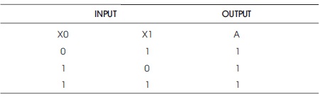
Table 1. Truth Table of 2x1 Encoder
The proposed encoder consists of an array structure of 37x31 rods in air. The refractive index is 3.45, lattice constant 'a' is 580 nm and radius of rod is 116 nm that is represent r=0.2*a. The proposed 2x1 encoder design is constructed by point and line defects. Line defects are defined waveguides of the structure, which is changing structural parameters of rods in row or column of the structure. Point defect is depends on function of change radius and refractive index of the rods. For the analysis performance of device, two methods are used in photonic crystal. One is FDTD method, which is used in computing electromagnetic wave distribution of the structure. And another method is PWE, which is used in analysing band structure for guided mode propagation in the design. Figure 2(a) represents band structure of propagated with range of 0.284 < a \ λ< 0.463 in TE mode propagation, λ is a wavelength of electromagnetic wave. Photonic band gap is accounted in range of 1252 nm<λ<2042 nm. Figure 2(b) shows PBG for introducing point and line defects. After introducing defects in this proposed structure, the guided modes are propagated in this region of PBG, which confines the signal in resonant wavelength of proposed 2x1 encoder design.
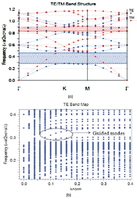
Figure 2. Band Structure of Proposed 2x1 Encoder Design (a) without Defects (b) with Point and Line Defects
The proposed 2x1 encoder design has two input waveguides and one output waveguide. Output waveguide is Y shaped waveguide. The waveguides are connected to the point defects of rods for signal propagation. Figure 3(a) represents schematic structure of 2x1 encoder design. Point defects are created by changing radius and refractive index of the rods, which is used to the purpose of coupling the signal into output waveguide of the proposed structure. And Figure 3(b) shows 3D structure of proposed 2x1 encoder with optimized size of footprint is 85 μm2.
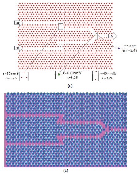
Figure 3. (a) Schematic Structure of 2x1 Encoder and (b) 3D Structure of Proposed Encoder Design
Two input waveguide are connected to the Y shaped waveguide with point defect for radius and refractive index of rod is 30 nm and 3.26, respectively. And the Y shaped output waveguide having three different point defects, where defects are mentioned in different colors for above proposed schematic structure. Green color of centre rod radius as 100 nm with refractive index of 3.26 and bending of Y shaped waveguide in two corners of block color rods kept radius is 40 nm and refractive index of 3.26. And the centre rod of blue color rod in output port Y shaped waveguide is denoted by 50 nm radius and 3.45 of refractive index.
When the input signals are applied in input ports of encoder, at the time simulation are started. The behavior of simulation fully depends on truth table of encoder. This field distribution of simulation process is used to analyze performance of encoder design with essential parameters of normalized power, contrast ratio, response time and bit rate. Any one input of X0 or X1 and both inputs of X0 and X1 is ON, output A is ON. Figure 4 represents field distribution for different logic of 2x1 encoder for (a) X0=0, X1=0 and A=0, (b) X0=1, X1=0 and A=1, (c) X0=0, X1=1 and A=1, and (d) X0=1, X1=1 and A=1. It is expressed that if any one input is active the output is enabled.
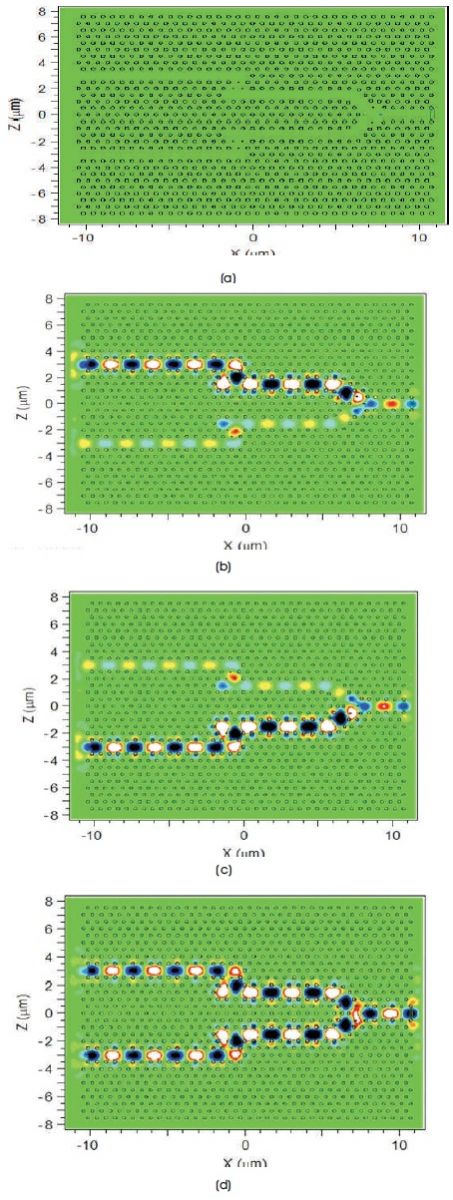
Figure 4. Field Distribution of 2x1 Encoder Design (a) X0=1, X1=0 and A=1, (b) X0=0, X1=1 and A=1 and (c) X0=1, X1=1 and A=1
Based on different logic function, the encoder design provides different performance depending on power efficiency. And the time evaluation curve shows normalized power level for different logic functions. Figure 5 shows output response of 2x1 encoder. It is used to find parameter of normalized power level, contrast ratio, response time, and bit rate.
Input signal is not given to both input ports that mean X0 and X1 is OFF, the device is not ON. In this OFF state, the device cannot couple any power. So we assume power level of 0.1% in logic 0 function. When the input is given to the input port X0, power will be coupled and the output port A is ON. For the second case of logic, the input port of X1 is activated which provides the output port enabled with greater than 73% power level. When both input ports of X0 and X1 is having input signal, the output port A is ON and maximum power level is provided in the encoder design.
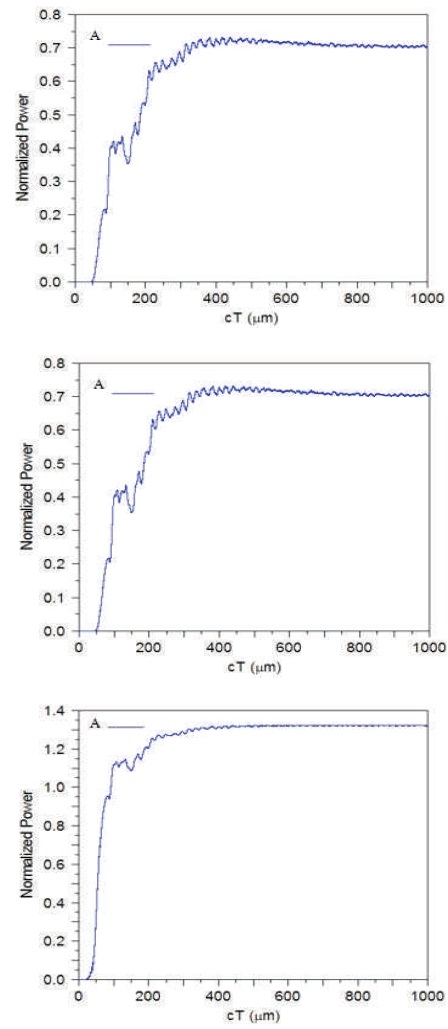
Figure 5. Output Response of 2x1 Encoder (a) X0=0, X1=0 and A=0, (b) X0=1, X1=0 and A=1, ( c) X0=0, X1=1 and A=1 and (d) X0=1, X1=1 and A=1
The proposed encoder provides the normalized power of 73% for logic 1 and 0.1% for logic 0. Response time is defined as the system to take time to reach maximum power at simulation. In this 2x1 encoder design, the average power at logic 1 of time t=1.2 ps (cT=380 μm) and the power reach at 10% with delay of time t1=0.21ps (cT=64 μm). The power level reaches at 10% to 90% of the average power t2 =0.99 for the narrow pulse, time is required t2=1.98 ps. And the response time of the signal propagation is 3.9 ps. The bit rate depends on response time of signal and it offers bit rate for 0.25 Tbps. Contrast ratio of design is described logarithmic with ratio is obtained by minimum ON to OFF logic level. Power level at logic 0 is approximately 0.001 and the power level of logic 1 is 0.73 (73%) for the contrast ratio 28 dB. Performance evaluation for different parameter analysis in 2x1 Encoder design is shown in Table 2. In this paper performance evaluation of output response is used to obtain parameter for normalized power, contrast ratio, response time, and bit rate. And it used to analyze the suitable features of encoder design.
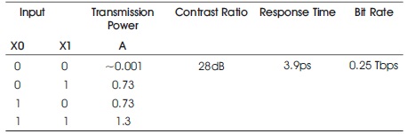
Table 2. Transmission efficiency, Contrast ratio, Response time and Bit Rate of 2x1 Encoder for Four Different Inputs
Table 3 shows the parameters comparison for different encoder design. In this proposed 2x1 encoder, it has high normalized power efficiency and high contrast ratio compared to another logic gates designs. Hence it could be suitable for real time applications in photonic integrated circuits.
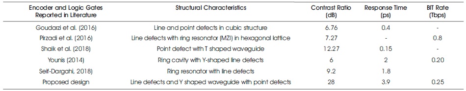
Table 3. Performance Comparison of Proposed Encoder with Reported PC Based Encoders
The proposed photonic crystal based Y shaped 2x1 encoder design offers 73% power level for logic 1. The functional parameters of contrast ratio, Response time, and Bit rate are analyzed. And the proposed design provides values of contrast ratio, response time, and bit rate of 12dB, 3.9 ps, and 0.25 Tbps, respectively. The point and line defects in the proposed encoder structure, is reduced power loss of coupled output ports. This encoder design is suitable for high speed of optical device of photonic integrated circuits for feature of high contrast ratio and compatibility.