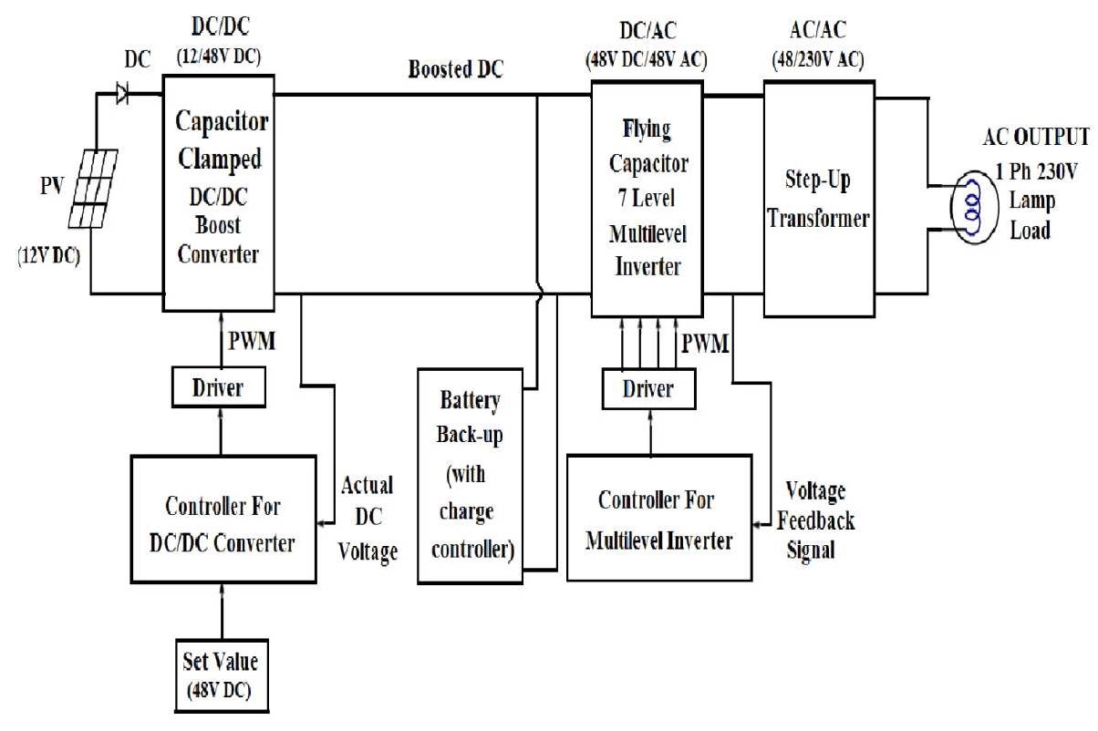
Figure 1. Overall Block Diagram of Proposed System
This paper concentrates on the closed loop control scheme, focusing on the reduction of Total Harmonic Distortion (THD) in a proposed seven level Flying Capacitor Multilevel Inverter (FCMLI). Among the various Multilevel Inverter (MLI) topologies, FCMLI provides more advantages. The development of closed loop model for seven level FCMLI dramatically reduces the low-order harmonics and THD. Extensive simulation has been applied to compare the performance of the proposed system in closed loop control scheme with that of the open loop control scheme. In order to justify the merits of the proposed system, it is interfaced with the single phase lamp load and analysed through simulation investigations.
With the increasing concern about the non-renewable energy sources, constant increase in the prices of fossil fuels, global warming and damage to environment and ecosystem, the renewable energy is becoming more popular and is gaining more attention as an alternative to non-renewable energy sources [1] . In Recent years, there has been an increasing interest in electrical power generation from renewable-energy sources, such as photovoltaic (PV) or wind-power systems [2] [3].
The benefits of power generation from these sources are widely accepted. They are essentially in exhaustible and environmentally friendly. Among the different renewable-energy sources possible to obtain electricity, solar energy has been one of the most active research areas in the past decades, both for grid connected and stand-alone applications [4] [5].
Multilevel power converters have become increasingly popular in recent years due to their high-power, high voltage capacity, low switching losses and low electromagnetic concerns. Nowadays different topologies have been reported for multi-level inverters. They are named as neutral point clamped (diode-clamped) inverter, flying capacitor (capacitor-clamped) inverter and cascaded multi-cell with separated DC source inverter [6].
In this paper, proportional-integral-derivative (PID) controller based closed loop system for seven level FCMLI and for capacitor clamped DC/DC boost converter have been developed. This scheme maintains the output voltage stability, reducing the harmonic content in the output there by improving the overall system performance. Through the proposed system, THD can be significantly reduced which is confirmed through simulation investigation.
Section 1 of this paper describes the architecture of proposed system, section 2 deals with the simulation model of proposed system and section 3 focuses on capacitor clamped DC/DC boost converter along with its configuration, description and significance of usage. Section 4 proposes the FCMLI topology with its merits and features and section 5 provides the performance of the closed loop system and the simulation results compared with the open loop system.
For this proposed topology, DC input to the system is a solar energy which is harvested from the Sun based on the irradiation and insolation level. In this system a single stand-alone PV module of 12V capacity is used to obtain the DC voltage. Then this obtained DC voltage is given as the input to the Capacitor Clamped DC/DC Boost Converter. By the DC/DC boost converter topology, the 12V DC is boosted-up to 48V DC. It is illustrated in Figure 1.
In order to maintain the constant DC voltage from the boost converter, a closed loop block is designed in which the actual DC voltage is compared with the 48V DC set value. Based on the error signal from the comparator, the PID controller produces the control signal to the PWM pulse generator block.
Then based upon the specified switching frequency of MOSFET, switching pulses are given to the single switch in the proposed DC/DC boost converter. Then the boosted DC voltage is given as the input to the seven level FCMLI which is intended for 48V DC to 48V AC conversion.
For controlling the FCMLI, a closed loop block is designed which consists of voltage measurement, voltage controller - PID controller and Sin generator block. With the help of these blocks, a closed loop design is achieved for proposed FCMLI. Then this low voltage AC signal of 48V AC is given to the step-up transformer for stepping up the voltage level to 230V AC. Finally a resistive load – single phase lamp load is connected across the 230V AC output terminals.
In order to feed the load continuously without any interruption, a battery back-up with charge controller unit is used in-between the DC/DC boost converter and FCMLI blocks.
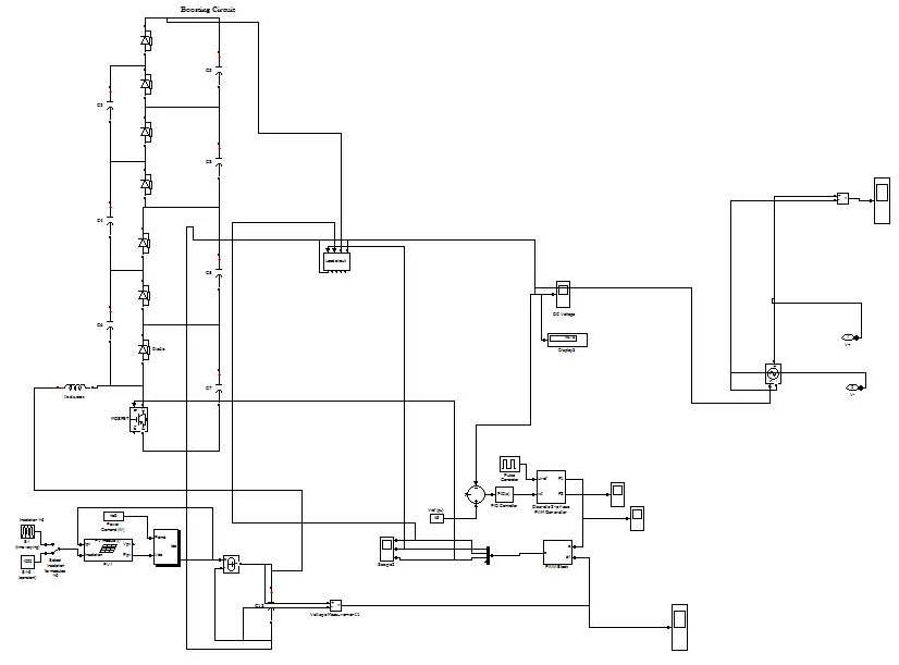
The overall simulation diagram of proposed closed loop system for FCMLI is illustrated in Figure 2.
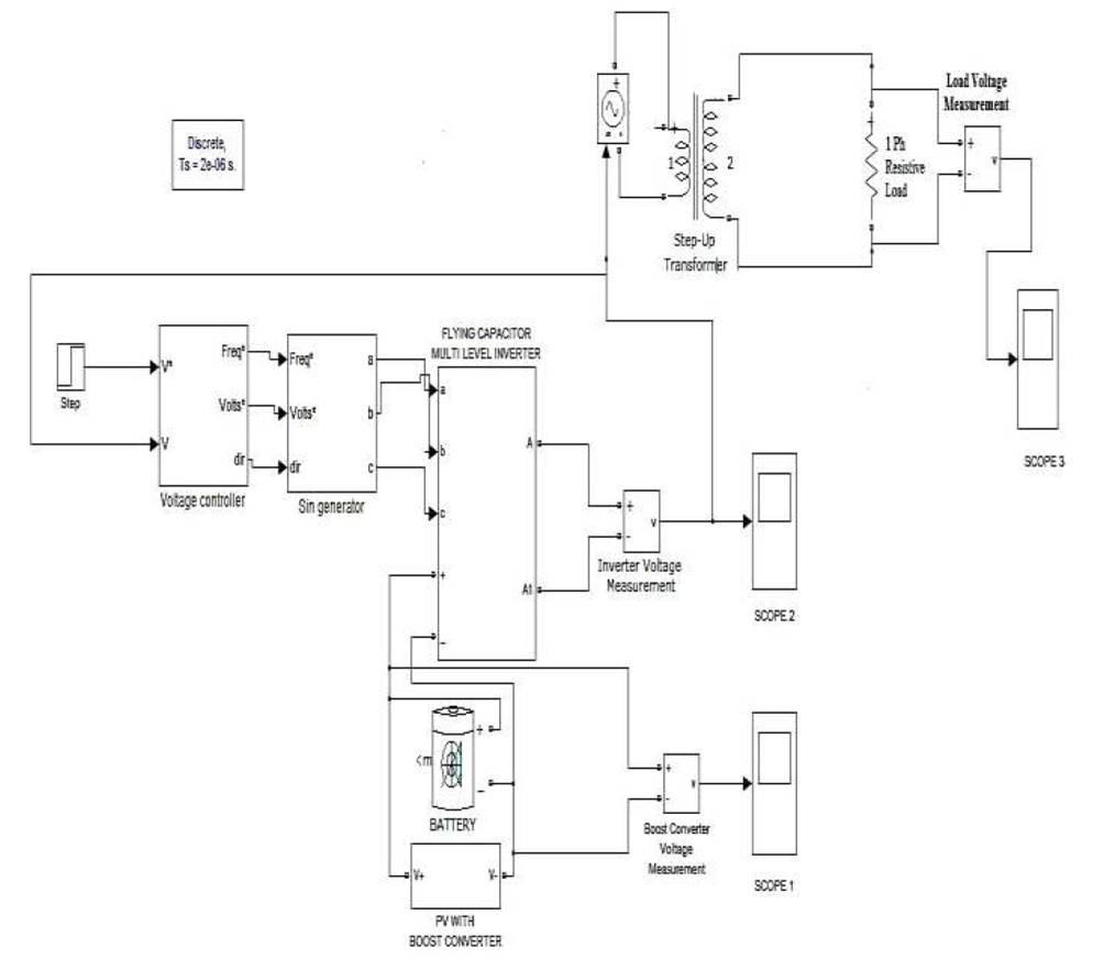
In the simulation model, various simulation blocks are used for accomplishing the required task in the proposed system. The appropriate functions of each block are as follows,
High-Power DC/DC converters are a crucial component of today's emerging vehicular technologies, such as hybrid-electric, battery-electric, and fuel-cell vehicles. Typically, a voltage boost is required to step up the low voltage of the fuel cell or battery to the required high voltage levels.
In these applications, it is imperative that the size and mass of the converter are reduced to facilitate packaging due to higher power density. Furthermore, the converter should feature a simple design with high-efficiency operation over the entire load range. In recent years, a number of circuits and control techniques have been proposed to reduce the switching losses in DC/DCboost converters [7].
In this paper, a capacitor clamped DC/DC boost converter topology is proposed. With this circuit topology, a low voltage DC from PV panel is boosted-up to the required level in a single stage since it employs a single MOSFET as the switching device. Due to this, the switching and conduction losses are reduced to the great extent. It is illustrated in Figure 3.
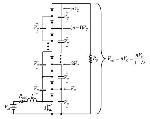
Figure 3. Basic Configuration of Capacitor Clamped DC/DC Boost Converter for Nx or N+1 levels
The proposed circuit is based on the multilevel converter principle, where each device blocks only one voltage level achieving high-voltage converters with low-voltage devices. It is a Nx DC/DC converter based on one driven switch, 2N+1 diodes and 2N+1 capacitors. One advantage of this topology is that the number of levels can be extended by only adding capacitors and diodes and the main circuit does not need to be modified.
The DC–DC Multilevel Boost Converter (MBC) is a PWM based DC/DC converter, which combines the boost converter and the switched capacitor function to provide different output voltages and a self-balanced voltage using only one driven switch, one inductor, 2N-1 diodes and 2N-1 capacitors for an Nx MBC.
The difference between the MBC and the conventional one is that in the MBC, the output is Vc times N, where N+1 is the converter's number of levels taking into account the zero level as illustrated in Figure 3. This behavior is achieved, thanks to the voltage multiplier in the boost converter's output that is driven by the only switch in the converter.
A Capacitor Clamped DC/DC Boost Converter with single switching element - MOSFET is proposed in this paper. Instead of using two or more than two number of switching devices as in the case of conventional half-bridge or full-bridge DC/DC converters, the proposed topology uses only one switching device there by fast switching with less switching loss is possible with this type of converter.
MLI is based on the fact that sine wave can be approximated to a stepped waveform having large number of steps. The steps being supplied from different DC levels are supported by series connected batteries or capacitors. The unique structure of MLI allows them to reach high voltages and therefore lower voltage rating device can be used. As the number of levels increases, the synthesized output waveform has more steps, producing a very fine stair case wave and approaching very closely to the desired sine wave. It can be easily understood that as motor steps are included in the waveform the harmonic distortion of the output wave decrease, approaching zero as the number of levels approaches infinity.
Hence MLI's inverters offer a better choice at the high power end because the high volt- ampere ratings are possible with these inverters without the problems of high dv/dt and the other associated ones [8].
Among the various MLI topologies, the FCMLI does not require isolated DC sides and additional clamping diodes, the snubber-less operation is possible and it is easy to be expanded to the multilevel. The FCMLI offers a great advantage with respect to the availability of voltage redundancies.
This inverter uses capacitors to limit the voltage of the power devices. They are defined as different combinations of capacitors allowing the charging or discharging of the individual flying capacitors in order to produce the same phase leg voltage. This advantage provides the special opportunity for controlling the individual voltage on flying capacitors [6] [9]. Many studies have shown that under certain conditions, a simple open loop control guarantees natural balancing of the flying capacitor.
The FCMLI requires a large number of capacitors to clamp the device (switch) voltage to one capacitor voltage level. Provided all the capacitors are of equal value, The size of the voltage increment between two consecutive legs of the clamping capacitors defines the size of voltage steps in the output waveform, if the voltage of the main DC-link capacitor is Vdc the voltage of the innermost capacitor clamping the innermost two devices is Vdc/(n-1).The voltage of the next innermost capacitor will be Vdc/(n-1) + Vdc/(n-1) = 2 Vdc/(n-1) and so on. Each next clamping capacitor will have the voltage increment of Vdc/(n-1) from its immediate inner one. The voltage levels and the arrangements of the flying capacitors in the FCMLI structure assures that the voltage stress across each main device is same and is equal to Vdc/(n-1) for an n- level inverter.
For a three phase inverter, two more legs of same construction are coupled to the same DC-link battery Vdc. In Figure 4 each switch SA1 to SA6 and S'A1 to S'A6 consists of a power semiconductor device (e.g. GTO, IGBT) and an anti-parallel diode. Voltages VC, Vc2, Vc3, Vc4, Vc5, and Vc6 are Vdc, 5/6 Vdc, 2/3 Vdc, Vdc/2, Vdc/3, and Vdc/6 respectively, as n = 7.
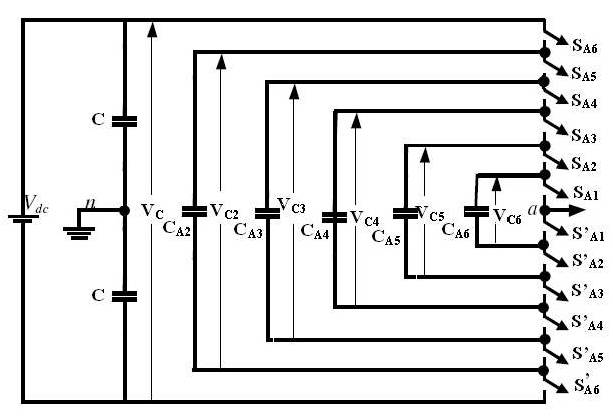
Figure 4. One Phase Leg of a Seven Level FCMLI
Large amount of storage capacitors can provide capabilities during power outages. These inverters provide switch combination redundancy for balancing different voltage levels. Like the diode clamp inverter with more levels the harmonic content is low enough to avoid the need of filters and both real and reactive power flow can be controlled.
In conventional method inverter cells are high. So the cost of the inverter is also high. The number of cells are high means the switching pattern of the inverter is difficult. In addition to the (n-1) DC link capacitors, the n level FCMLI with required (n-1)x(n-2)/2 auxiliary capacitors per phase, if the voltage rating of the capacitor indistinguishable to that of the main switches is high.
The main advantages of FCMLI are; real and reactive power flow can be controlled. Phase redundancies are available for balancing the voltage levels of the capacitors.
The FCMLI has the following features. They are,
The proposed topology of closed loop system for FCMLI consists of various models. They are,
The Simulation diagram for the PV Generation by a single stand-alone 12V PV module is illustrated in Figure 5.

Figure 5. MATLAB Model of Input PV Module
It consists of Insolation block, single PV module block for DC voltage generation, display and scope blocks for displaying the output in numerical and graphical form respectively. The technical specifications of the PV module used in the proposed system are listed in Table 1.
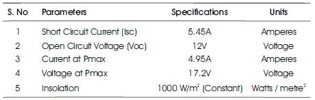
Table 1. Technical Specifications of PV Module
The Simulated output is taken for 1000 watts/m2 of Insolation and 25°C of Temperature under Standard Test Condition (STC).
The corresponding output voltage waveform of 12V PV Panel is illustrated in Figure 6.
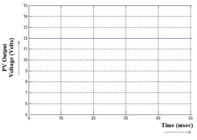
Figure 6. Output Voltage Waveform of PV Module
Thus from the PV Panel, a 12V DC of Unidirectional Voltage is produced. Then this low value of DC voltage is given to the Boost converter for achieving desired DC voltage for giving input to the Multilevel Inverter.
From the PV module a 12V DC voltage is obtained. This unidirectional DC voltage is then given to the Capacitor Clamped DC/DC Boost Converter for boosting up the voltage up to 48V DC.
The Simulation diagram of the Capacitor Clamped DC/DC Boost Converter is illustrated in Figure 7.
It consists of various circuit elements such as Boost Inductor, MOSFET, Clamping Capacitor and free-wheeling diodes for boosting up the DC voltage from PV panel – 12V DC into 48V DC. It also consists of a comparator, PID controller, pulse generator and PWM block for producing pulses for MOSFET.
The corresponding output voltage waveform of the proposed Capacitor Clamped DC/DC Boost Converter is illustrated in Figure 8.
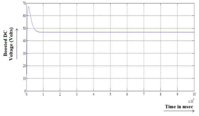
Figure 8. Output Voltage Waveform of Boost Converter Model
From the above output, the main inference is initially the voltage signal is raised to nearly 60V DC and then it is settled down to the 48V of DC. The reason behind that is because of the presence of the boosting inductor in the initial stage of boost converter, the voltage raise takes place and after that based on the set value in comparator it falls to actual pre-defined value.
From the Boost Converter Model, a 48V of DC is given to the Seven Level FCMLI for converting a DC voltage into stepped output waveforms.
Figure 9 illustrates the corresponding overall simulation model of proposed Multilevel. It shows the overall simulation model of proposed seven level FCMLI which includes the Inverter model and pulse generation model.
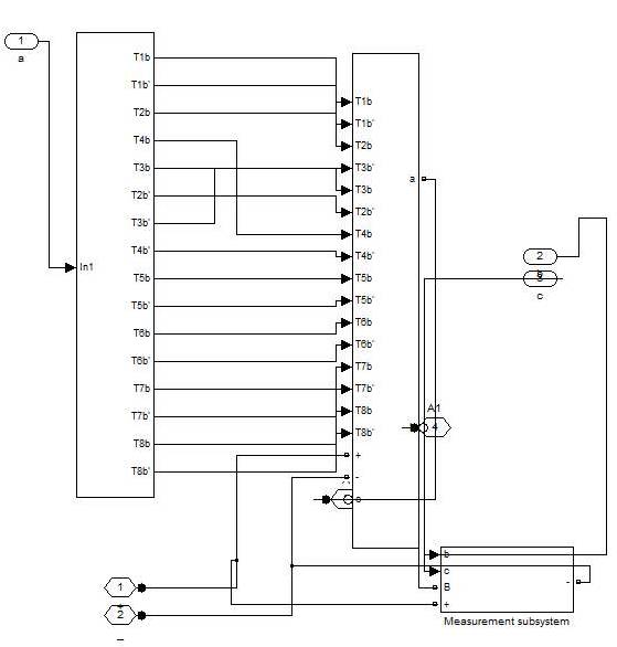
Figure 9. MATLAB Model of seven level FCMLI
The proposed seven level FCMLI will produce the seven level of stepped AC output waveforms at its output. The switching sequence of various switches used in the Inverter model are determined by the PWM pulses from the pulse generation model.
Here Multicarrier PWM in turn of PD-PWM technique is employed for generating appropriate PWM pulse signals for respective switches in the MLI. Figure 10 illustrates the Pulse Generation Model Using Multicarrier PWM – PDPWM technique for Seven Level FCMLI.
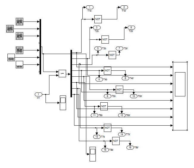
Figure 10. Pulse Generation Model for FCMLIUsing Multi carrier (PDPWM) Technique
In this Pulse Generation Model, there are six number of carrier signals which are produced by Repeating sequence concept and these signals are compared with the Sinusoidal signal with the help of the relational operator (>=).
Figure 11 illustrates the comparison of six numbers of carrier signals and the sinusoidal modulating signal. In which the sinusoidal signal is superimposed over the carrier signals for generating appropriate PWM pulses.
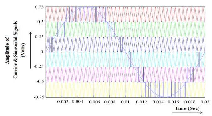
Figure 11. PDPWM Modulation Scheme
The Simulation is taken for the seven level FCMLI with Multicarrier Pulse Width Modulation Technique. The corresponding open loop output voltage waveform of proposed FCMLI is illustrated in Figure 12.
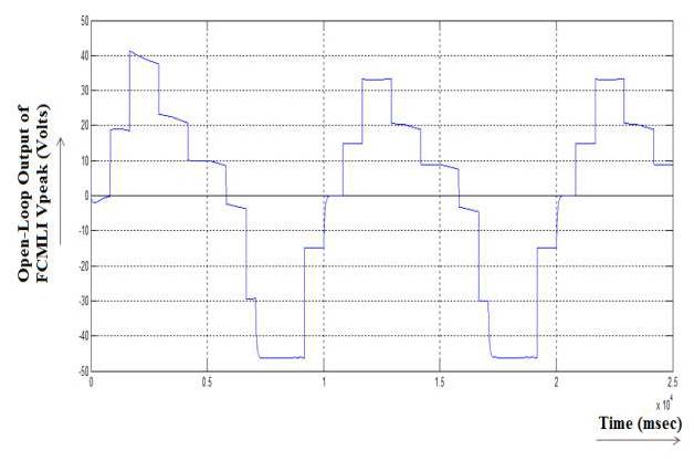
Figure 12. Open Loop AC Stepped Output Voltage Waveform of FCMLI
From the Open loop output, it is observed that seven level stepped output waveform with the magnitude of nearly 48V is achieved but it is slightly distorted. Because of this the THD of open-loop output is having more percentage values.
Thus in order to reduce the THD level of Multilevel Inverter output and to improve the performance of the system, a closed-loop design is essential for Multilevel Inverter. By implementing the closed-loop system, the THD level can be reduced to certain extent.
In order to reduce the THD level of MLI output a closed-loop model was developed and its corresponding output voltage is illustrated in Figure 13.
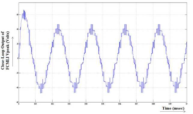
Figure 13. Closed Loop AC Stepped Output Voltage Waveform of FCMLI
From Figure 13, it is clear that the AC output voltage waveform of closed loop model is more sinusoidal with more precise steps.
Figure 14 illustrates the corresponding output voltage waveform of a step-up transformer (48/230V AC). This AC voltage is fed to the Single Phase Lamp Load.
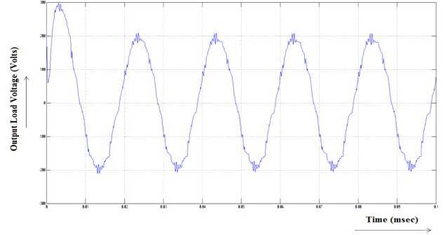
Figure 14. Output Load Voltage Waveform of Proposed System
The Total Harmonic Distortion (THD) is used to characterize the linearity of audio systems and the power quality of electric power systems.
The formula below shows the calculation for THD on a voltage signal. The end result is a percentage comparing the harmonic components to the fundamental component of a signal. The higher the percentage, the more distortion that is present on the mains signal.

The results of THD analysis performed for both open-loop and closed-loop systems are illustrated in Figures 15 and 16.
From Figure 15, it is observed that the THD value of 37.15% is obtained for Open-Loop FCMLI system. This value can be reduced by Closed-Loop design.
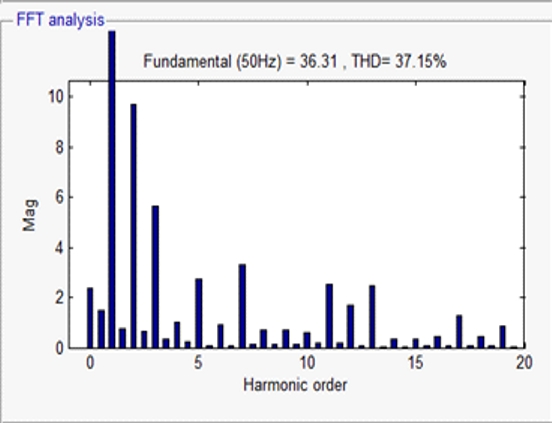
Figure 15. Open-Loop THD Result of Seven Level FCMLI
The result of THD analysis performed for Closed-Loop system is illustrated in Figure 16.
From Figure 16, it is observed that the THD value of 10.18% is obtained for Closed-Loop FCMLI system. This is comparatively lesser value than the THD obtained in Open-Loop system.
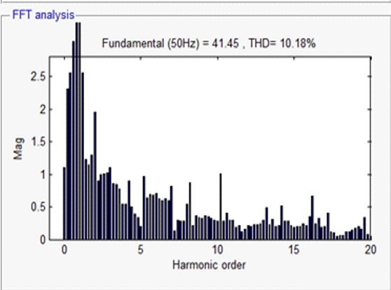
Figure 16. Closed-Loop THD Result of Seven Level FCMLI
In the proposed method, a closed-loop system was implemented for a Seven Level FCMLI. The newly developed design will improve the system performance and maintains the voltage stability and there by stable operation can be ensured without more disturbances. The closed loop controller is also designed for Capacitor Clamped DC/DC Boost Converter there by constant output voltage at the output of the boost converter can be achieved.
The performance was verified through simulation models by using MATLAB software tool. From the simulation study, the important conclusions are,
The main inference from the proposed concept is, for the developed Seven Level FCMLI system, the THD value of open-loop model is 37.15% and for the closed-loop model it is 10.18%. Thus the percentage of THD value can be minimized by implementing the closed-loop control for FCMLI and there by better performance in its output can be achieved.