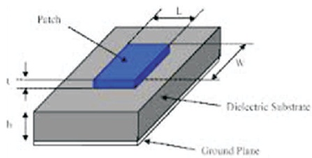
Figure 1. Structure of a Microstrip Patch Antenna
A novel approach to design a microstrip patch antenna is proposed for wide beam and low profile applications. In this research work, microstrip patch antenna is structured to compose X-shaped cut on rectangular patch. The need of high data rates for wireless communication becomes more and more urgent, and various solutions have been brought forward. This X-shaped microstrip patch antenna is an excellent design for ultra wide band applications. The proposed antenna simulation is going to be carried out through 3D electromagnetic simulation software called ANSOFT HFSS and fabricated on dielectric substrate FR-4 by using Microstrip line feeding technique. Using Vector Network Analyzer E5071C, the invent antenna is tested and results are to be differentiated with Simulation results. The parameters that are focused here is resonant frequency, return loss, VSWR, Gain, and Percentage Bandwidth.
The Federal Communication Commission (FCC) releases ultra-wide band (UWB) from 3.1-10.6 GHz in 2002 for the use of indoor and hand-held systems. UWB antennas have extensive recognition in both study, research, and production for applications in wireless transmission systems. An UWB system sends very low power pulses, below the transmission noise threshold (Rahim, Karim, Masri, & Asrokin, 2007; Badjian, Chakrabarty, Hock, & Devkumar, 2008). Impulse-Ultra wideband (I-UWB) is a small carrier tiny sweep communications technology in which its transference inhabited a bandwidth of more than 20% of its center frequency (>500 MHz) (Brzezina, Ye, & Roy, 2005). Antenna also plays an essential role in UWB systems. Ideally, the UWB antenna should be compact, planar, low cost, and reliable (Ping, Chakrabarty, & Khan, 2010). From a systems way of considering a matter, the response of the antenna should overspread the entire operating range of frequencies, and the antenna should be non-receptive to signals beyond the limits of the stated band (Kumar, Basu, & Koul, 2011). A directional antenna concentrates the energy into a narrow solid angle compared with an omnidirectional antenna; and generally, it requires being relatively large compared to the omni-directional one. Before the 1990's, all the proposed UWB antennas were based on general volumetric structures (Schantz, 2004). UWB have more uses in short range and high speed wireless systems, such as ground pungent radars, medical imaging system, high data rate wireless local area networks (WLAN), communication systems for military and tiny pulse radars for automotive even or robotics. The antenna is one of the crucial components, which determine the performance of UWB system (Azim, Mobashsher, Islam, & Misran, 2010). To tackle the effect caused by the frequency interference from WLAN (5.15–5.825 GHz) and WiMAX (5.25–5.85 GHz) systems, some UWB antennas with band-notched feature have been designed (Liu, Ku, Wang, & Yang, 2010). In the past, one serious limitation of the microstrip antenna was its narrow bandwidth characteristics, being 15 to 50% that of commonly used antenna elements such as dipoles, slots and waveguide shorns (Peyrot-Solis, Galvan-Tejada, & Jardon-Aguilar, 2005). This restriction was successfully detached achieving a matching impedance bandwidth ratio it was necessary to increase the size, height, volume, or feeding and matching techniques (Garg, Bhartia, Bahl, & Ittipiboon, 2001) in general, UWB communication antennas need low voltage standing wave ratio (VSWR<2), constant phase center, constant group delay, and constant gain over entire operating range of frequency band (Sobli & Abd-El-Raouf, 2008).
In the wide range of antenna models, there are different structures of Microstrip antennas, but on the whole we have three basic parts in the antenna as shown in Figure 1.
They are:
The structure of Microstrip Patch Antenna is present in the following figure (Figure 1).
Figure 1. Structure of a Microstrip Patch Antenna
Open-circuit walls on the sides. In a cavity, only certain modes are allowed to prevail, at dissimilar resonant frequencies. If the antenna is stimulated at a resonant frequency, a strong field is set up inside the cavity, and a strong current on the (bottom) surface of the patch. This produces significant radiation, which makes a good antenna.
The base configuration of the X shaped slotted compact antenna is manufactured on a dielectric substrate having a relative dielectric constant €r = 4.4 and thickness 1.6 mm as shown in Figure 2. This is the reference antenna or base shape patch antenna. The width and length of the base shape are a = 38 mm and b = 30.1 mm, respectively.
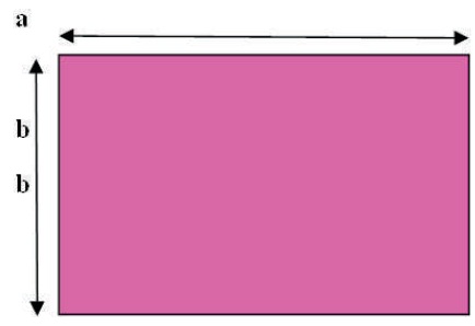
Figure 2. Geometry of Base Shape Patch Antenna
For the X shape, slot is cut inside the geometry of base shape patch antenna in Figure 3.
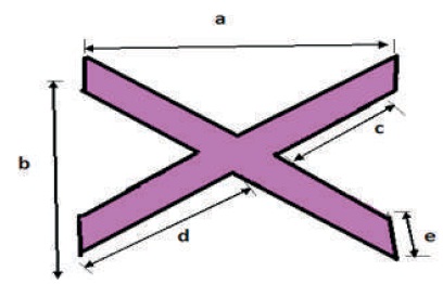
Figure 3. Geometry of X Slot on the Patch
The total length and width are a = 32 mm and b =23 mm, respectively. The optimized design dimensions are a = 32 mm, b = 23 mm, c = 12 mm, d = 13 mm, and e = 4 mm. A 50 ohm SMA connector is used to feed the antenna by using microstrip line feed technique (Figure 4).
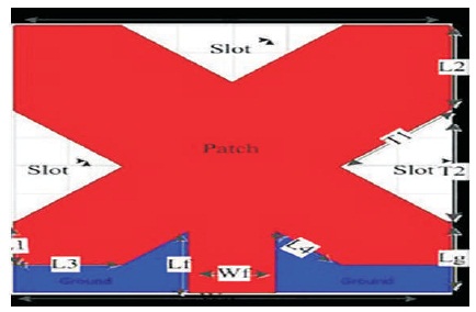
Figure 4. X Shape Compact Antenna with Microstrip Line Feeding Technique
The design of a Microstrip Patch Antenna involves the following steps:
The proposed antenna is simulated in ANSOFT HFSS software and the results obtained are shown in below figures (Figures 5-8).
These figures give the simulated return loss characteristics. From different measures proposed before by various studies, the antenna will respond to certain frequencies, where the return loss is less than -10 dB. The response is shown below of the designed antenna, where the x shape antenna is operated at two bands of frequencies at 3.8 GHz and 6.2 GHz with Return loss -19.1 and -21.4, respectively, which is the simulated VSWR characteristics, where the VSWR is minimum i.e., 1.1 dB and 1.2 dB at resonant frequencies.
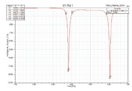
Figure 5. Simulated Returnloss Characteristics (in ANSOFT HFSS)
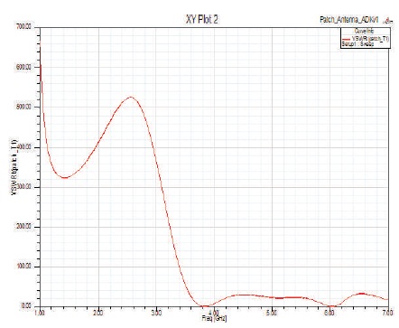
Figure 6. Simulated VSWR Charecteristics (in ANSOFT HFSS)
The proposed antenna is fabricated and its practical results are obtained using Vector Network Analyzer (VNA)- E5071C, and the results are shown below.
The Figure 7 shown below is the proposed antenna with Microstripline feed technology has been used in dual band operations. The proposed dual band antenna consists of a rectangular shaped patch element embedded with X shaped slot in the middle of the patch element, capable of generating two separate bands with good impedance matching conditions.
Figure 7 shows the resonanant frequency and return loss values of X shape antenna at practical measurements, where the X shape antenna is operated at two bands of frequencies at 3.81 GHz and 6.03 GHz with return loss - 19.1 and -21.3, respectively (Table 1).
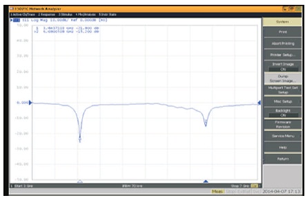
Figure 7. Return Loss in Db Curve (in VNA)
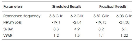
Table 1. Results of Parameters at Two Resonant Frequencies
The above shown Figure 8 are obtained when the proposed antenna is tested by using the Vector Network Analyze r(VNA)-E5071C. Figure 8 shows the VSWR values for X shape antenna at practical conditions, where the X shape antenna is operated at two Frequencies, which have lower VSWR value (Table 2).
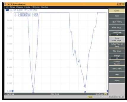
Figure 8. VSWR Curve (in VNA)
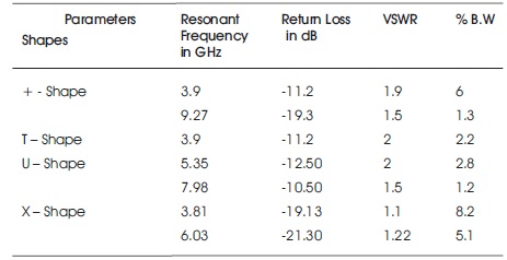
Table 2. Comparison of Antenna Parameters with Different Patch Shapes
An X shaped compact patch antenna is designed for dual band applications in satellite communications. The various parameters of the proposed antenne are optimised through simulation. Prototype of the proposed antenna has been designed, simulated, and fabricated.
Here the antenna is operated in the range of 3.2-6.5 GHz. So it is widely used in dual band frequencies that means single antenna is operated and responded efficiently at two frequencies. So it will be useful for two applications simultaneously by a single antenna.
During antenna simulation and fabrication, many problems appear. One of the problems in this work is related with the substrate thickness t, where the substrate height was considered in the simulation as 1.6 mm, but the thicknesses of patch, strip line, and ground were not considered, and they were all 0.035 mm. Then, in simulation result for return loss S11, the resonant frequency has been shifted from 3.8 to 6.0 GHz. After many steps in simulation and fabricating more than three antennas, the problem has been solved, being about the thickness of patch and ground.
In future Work, one may modify any antenna shape to a specific application. Future work will concentrate on how to tackle with size and performance of these types of antennas. Triple band with high gain will be a good idea to continue studies in this field.