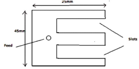
Figure 1. Probe Feed E-shaped Patch Antenna
The objective of E-shaped patch antenna with hexagonal slot is to operate in the ISM band for different kind of applications, such as WLAN, GPS, and various modern wireless systems. The posit antenna is designed using FR4 substrate having a dielectric constant of 4.4 with a thickness of 1.6 mm. Probe feed technique is used for this antenna design. A parametric study was included to determine the effect of design approaches and the antenna performance. The realization of the designed antenna was analyzed in term of boost (gain), return loss, and radiation pattern. The design was upsurged to confirm the best achievable result. This antenna resonates at three different frequencies at 1.6 GHz, 3.24 GHz, and 5.6 GHz with a reflection coefficient less than -10 dB and VSWR<2.
Antenna is a type of transducer which is used to convert electrical energy, into RF energy. Antenna is a basic device for any communication setup. The basic structure of patch antenna consists of dielectric substrate sandwiched between metal patch on one lateral and metal ground plane on the other side. A microstrip or patch antenna is a small profile that has a more advantages than other antennas. It is shiny loaded, low cost, and accessible to combine with accompanying electronics. While the antenna can be 3D in structure, the components are usually flat, hence their alternate name, planar antennas. A planar antenna is not always a patch antenna. The interior conductor of a coax handles as a feed probe to set electromagnetic energy in and / or out of the patch. The electric field is zero on the inside of the patch, maximal (positive) and one side, and mere (negative) on the other side. It should be that the maximum and minimum regularly change side, according to the rapid phase of the applied signal.
The proposed design is mainly concentrated on the respective parameters, such as gain, VSWR, return loss, and radiation pattern. Coming to a brief description about all the parameters, for every 6 dB the gain will be improved as like as double the range of the antenna and its improves the efficacy.
Similarly, VSWR is used to measure the impedance matching to the respective radiating signal, for the purpose of minimal VSWR. With the lesser VSWR to give better directivity and improve the power handling mechanism of the antenna. Whenever the VSWR is occurred below the unity level, at that time no power is getting back to the respective antenna. Due to which we can avoid the return loss in the antenna ultimately improves the gain of the particular antenna.
The main motto of this design is to improve the gain of the system as well as reduce the return losses at multiple bands for various wireless applications. Particularly this system operates at 1.6 GHz, 3.2 GHz, and 5.6 GHz ranges; in this range the authors obtain the results and verified.
Most of the past, researchers are focusing on the gain and power factors in the antennas using multiband conditions (Kumar, Gupta, Marriwala, & Tripathi, 2011; Moernaut & Orban, 2006), operated at 1-6 GHz with compact radiation. E shaped patch antenna (Yang, Zhang, & Rahmat-Samii, 2001; Banuprakash, Amith, Gagana, Ravi, & Pavanashree, 2018) designed with a frequency 1.9 GHz and 2.4 GHz for achieving the wide bandwidth. The shape will provide the broad bandwidth for wireless communication systems (Verma, Verma, & Dhubkarya, 2009; Ayoub, 2003). To measure different parameters, a low dielectric constant and considerable losses for Eshaped patch in C-band are considered (Vetharatnam, Chung, & Chuah, 2005; Ge, Esselle, & Bird, 2004). For good impedance matching over a wide bandwidth, simply, we can insert a pair of wide slits on a radiating edge (Wong, & Hsu, 2001). The E-shaped patch antenna implemented with corrugation into the two side wings (Ge, Esselle, & Bird, 2006; Yu, & Zhang, 2003), can reduce the size of the antenna as well as the gain, bandwidth without the use of parasitic patches (Lee et al., 1997; Rafi & Shafai, 2004) in the same layer. By selecting proper dimensions in the patch, we can obtain the dual frequency (Sim, Row, & Liou, 2007), with single feed. Simulation results are obtained from HFSS software.
In this multiband antenna, FR4 substrate of permittivity εr = 4.4 with length 25 mm, width 45 mm, and height 1.6 mm are considered. This substrate is sandwiched between the ground plane and patch. Two slots S1 and S2 are cut out from the patch near the feed line to match the impedance. The slots S1 and S2 are identical and equidistant as shown in Figure 1 and the hexagonal slot on E-shaped patch antenna is also represented in Figure 2.
Figure 1. Probe Feed E-shaped Patch Antenna
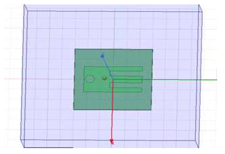
Figure 2. Simulation Prototype of E-shaped Patch Antenna with Hexagonal Slot
The proposed antenna was simulated using ANSYS HFSS simulation. In this proposed design, the authors have used a probe feeding technique with hexagonal slot. In coaxial probe feed, there are two materials, say inner and outer. The focal material is generally a conductor and it has touched the radiating patch. The exterior material is generally made of insulating material like Teflon and it touches the ground plane.
The antenna geometry is shown in Figure 3, where the antenna has only one patch, which is simpler than traditional multiband microstrip antennas. The patch size is characterized by (L, W, and H) and it is fed by a coaxial probe at position (Xf, Yf). To expand the antenna bandwidth, two parallel slots are joined into this patch and position equitably with respect to the feed point. The topological shape of the patch resembles the letter “E”, hence the name E shape patch antenna. The slot length (Ls), width (Ws) and position (Ps) are essential elements in supervising the obtainable bandwidth (Ge, Esselle, & Bird, 2004).
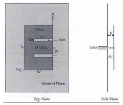
Figure 3. Geometry of a wide-band E-shaped Patch Antenna Consisting of Two Parallel Slots in the Patch
The main motto of the multiband mechanism of the E shape patch antenna. The ordinary microstrip patch antenna can be modeled as a simple LC resonant circuit. Current flows from the feeding point to the top and bottom edges. L and C values are determined by this current path length. When two slots are absorbed into the patch, the resonant feature changes, as shown in Figure 4. It produces the initial LC circuit and oscillates at the initial frequency. However, at the end part of the patch, the current has to flow around the slots and the period of the current path is increased. This effect can be modeled as additional series inductance ΔLs, so the equivalent circuit of the corner part oscillates at a minor frequency. Therefore, antenna changes from single LC resonant circuits to a coupled resonant circuit. These two resonant circuits couple together and form a large bandwidth.
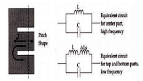
Figure 4. The E-shaped Patch Antenna
The main E shaped patch has Wa x La dimension. The antenna is fed by a SMA connector positioned at the center arm. The center of the probe is positioned at (Wc/2, Lf ). The width and length of the microstrip antenna are determined as follows.
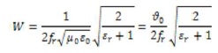
where νo is the free-space velocity of light.
The scale of the patch along its length have been extended two on each end by a distance ΔL, which is a behavior of the effective dielectric constant εreff and the width to height ratio (W/h), and the normalized extension of the length is
The actual length of the patch (L) can be determined as,
Equidistant slots in this design are responsible for the stimulation of next resonant mode, i.e. main parallel slot excites resonant frequency. Slot length (Ls), slot width (WS), and center arm (Wc) controls the frequency of the next resonant mode. Figure 4 shows the cut plane view of the antenna. The patch and ground are detached from closed-cell minimal defeat air and it benefits to obtain wider bandwidth and higher gain.
Figure 5 shows the flowchart of proposed system flow.
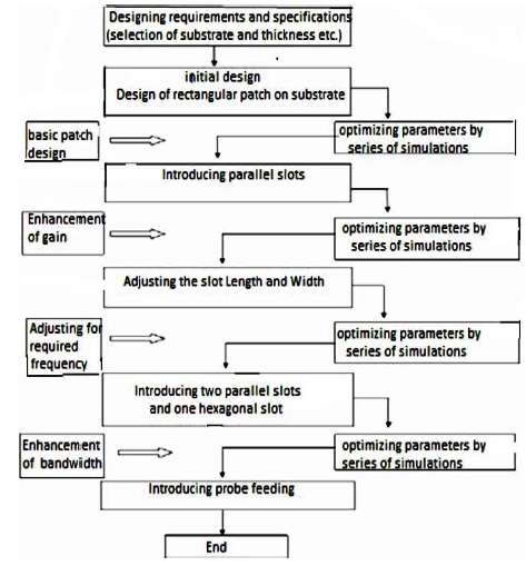
Figure 5. Flowchart
Table 1 shows the design parametric table.
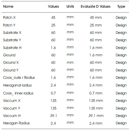
Table 1. Design Parametric Table
The simulation results are taken and verified at multiple frequencies. For each frequency, gain, VSWR and return losses are calculated and verified for the proposed antenna. Radiation pattern for Gain 4 dB, -2 dB, -10 dB at 1.98 GHz, 3.24 GHz, and 5.6 GHz are presented in Figure 6, respectively, similar the Return losses S11 is -35 dB at 5.6 GHz is shown in below mentioned Figure 7. The 3-D polar plots of the waveforms are presented at different range of frequencies. The simulations are obtained from the HFSS software.
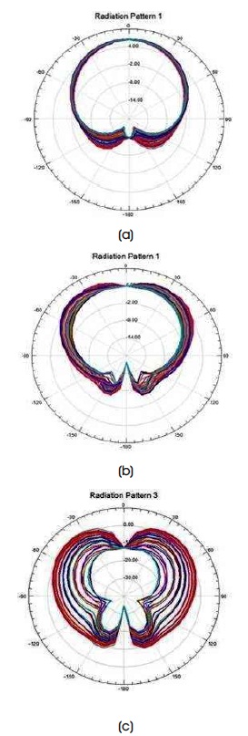
Figure 6. (a) Gain at 1.98 GHz (b) 3.24 GHz (c) 5.6 GHz
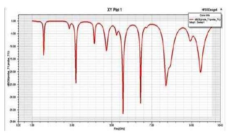
Figure 7. Return Losses
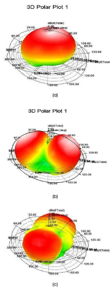
Figure 8. (a) Radiation Pattern at 1.98 GHz (b) 3.24 GHz (c) 5.6 GHz
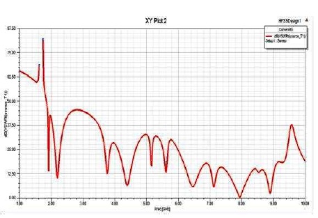
Figure 9. VSWR at 5.6 GHz
This paper concludes the design of E-shaped patch antenna with hexagonal slot for various wireless applications, such as WLAN, GPS, and different kinds of modern technology. The simulation results are obtained and verified at different range of frequencies like at 1.98 GHz, 3.24 GHz, 5.6 GHz for multiband purpose. With the aid of HFSS Simulation software, the results are obtained VSWR, for Gain, return loss, radiation patterns, and reflection coefficient at above mentioned frequencies.