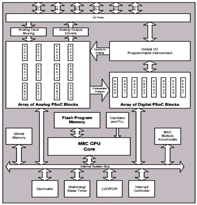
Figure 1. Architecture of PSoC Device
Programmable System on Chip (PSoC) devices are becoming forerunning technologies in the field of embedded systems design. The innovation of PSoC device comes from the user configurability of analog and digital array blocks. The Programmable System-On Chip devices are integrated with processors, memory, and peripherals to facilitate easy and modular design in building embedded applications. This paper describes in general about the PSoC device architectures and design of a test module using the PSoC device (CY8C26443) for testing the resources like Analog to Digital and Digital to Analog Converters (ADCs and DACs) of a microprocessor based embedded system.
Recent advances in programmable devices have provided a viable solution for rapid prototyping of complex systems focused primarily on digital programmable devices, such as Field-Programmable Gate Arrays (FPGAs), Complex Programmable Logic Devices (CPLDs), and reconfigurable processors. Discrete programmable analog arrays have also been released as products with limited acceptance (Mar, Sullam, & Blom, 2003; TRAC020LH Datasheet), due to their high price/performance ratio. High-volume consumer applications often make use of a small processor and peripheral devices that are implemented with a few offthe- shelf parts, and low analog price/performance ratios. Integration of programmable analog and digital peripherals with a microcontroller can facilitate the realization of low-cost single-chip embedded systems. Programmable System on Chip (PSoC) CY8C25XXX /CY8C26XXX families of devices are invented by M/s Cypress Microsystems. A PSoC device can replace multiple microcontroller based system components with a single configurable device (Documentation of PSoC designer software IDE). A single PSoC chip could replace nearly 10 to 15 discrete integrated circuits for medium to complex applications. Some of the advantages of using PSoC devices in place of traditional test systems using PC add-on cards are much less number of components and connections on the circuit board, choice in selecting the required hardware on the PSoC device, user can program the device with the available Integrated Development Environment (IDE), Emulator and programming environment for the PSoC device, flexibility in changing the device configuration with minimum changes on the circuit board, less development time, less cost, and lot of scope for implementing other applications.
The PSoC provides a micro-controller core, flash program memory, SRAM data memory, and configurable analog and digital peripheral blocks in a single chip. Unlike a traditional microcontroller, the digital and analog peripherals are field programmable. PSoC has 8 Digital blocks (4 with communications capabilities) and 12 Analog blocks (4 continuous-time type and 8 switchedcapacitor type). It operates from 96 Hz to 24 MHz CPU. Digital blocks can be configured as timers, controllers, or serial communications ports. Analog PSoC blocks can be programmed by setting a few registers to interconnect and trim the appropriate operational amplifier circuit to create the desired result (Rucinski, 2012). Among the typical peripherals that can be created are amplifiers, comparators, ADCs, DACs, and filters. Configurable- analog- module is one of the major advantages of this PSoC device. A PGA in PSoC can be configured to 31 different gains ranged from 0.063 to 16. The bandwidth of amplifier is 8.9 MHz and the settling time is 0.6 μs (Kane, 2012). The slew rate for the output with interconnection (20% - 80%) is 2 V/μs. When the output of PGA is connected to an external pin, an extra analog buffer delay will be introduced. PSoC provides 6-bit, 8-bit, 12-bit, and 7-13 variable bits ADCs. The 6-bit ADC is a SAR (Successive Approximation Register) converter and supports burst sample rates up to 45 KHz. The 12-bit ADC is a 12-bit incremental converter that supports sample rates from 7.8 sps (sample per second) to 488 sps. It is an integrating ADC that provides rejection of higher frequencies (Kane, 2012). The 8-bit ADC is a Delta-Sigma converter that supports sample rates from 1.8 ksps to 31 ksps. The sample rate is determined by the data clock input and is selectable by the user. The PSoC architecture overview is as shown in Figure 1.
Figure 1. Architecture of PSoC Device
PSoC blocks are user configurable system resources. On-chip digital and analog PSoC blocks reduce the need for many external peripheral components. Digital and analog PSoC blocks can be configured to provide a wide variety of peripheral functions (Lee & Gulak, 1991). PSoC Designer Software Integrated Development Environment (IDE) provides automated configuration of PSoC blocks by simply selecting the desired functions. PSoC Designer then generates the proper configuration information and can print device data sheet unique to that configuration. Digital PSoC blocks provide ADCs, multipurpose timers/ counters, Pulse Width Modulators (PWM), Programmable gain amplifiers, etc. In addition to all PSoC block functions, communication PSoC blocks support full-duplex UARTs and SPI master or slave functions. There are a total of eight 8-bit digital PSoC blocks in this device family configured as a linear array. Four of these are the Digital Basic Type A blocks and four are the Digital Communications Type A blocks (Data sheets of CY8C26443 PSoC device). Each of these digital PSoC blocks can be configured independently, or used in combination. Each digital PSoC block has a unique Interrupt Vector and Interrupt Enable bit. Functions can be stopped or started with a useraccessible Enable bit. The Timer/Counter/ CRC/PRS/Dead band functions are available on the Digital Basic Type A blocks and also the Digital Communications Type A blocks. The UART and SPI communications functions are only available on the Digital Communications Type A blocks. There are three configuration registers: the Function Register (DBA00FN-DCA07FN) to select the block function and mode, the Input Register (DBA00INDCA07IN) to select data input and clock selection, and the Output Register (DBA00OU-DCA07OU) to select and enable function outputs. The three data registers are designated Data 0 (DBA00DR0-DCA07DR0), Data 1 (DBA00DR1- DCA07DR1), and Data 2 (DBA00DR2- DCA07DR2). The function of these registers and their bit mapping is dependent on the overall block function selected by the user (Data sheets of CY8C26443 PSoC device). The one Control Register (DBA00CR0- DCA07CR0) is designated Control 0. The function of this register and its bit mapping is dependent on the overall block function selected by the user.
Analog blocks have many potential inputs and several outputs. The inputs to these blocks include analog signals from external sources, intrinsic analog signals driven from neighboring analog blocks or various voltage reference sources (Kanithkar, 2007). There are three discrete outputs from each analog block (there are an additional two discrete outputs in the Continuous Time blocks), 1) the analog output bus (ABUS), which is an analog bus resource that is shared by all of the analog blocks in a column, 2) the comparator bus (CBUS), which is a digital bus resource that is shared by all of the analog blocks in a column, and 3) the output bus (OUT, (plus GOUT and LOUT in the Continuous Time blocks)), which is an analog bus resource that is shared by all of the analog blocks in a column and connects to one of the analog output buffers, to send a signal externally to the device. There are also intrinsic outputs that connect to neighboring analog blocks (Millman & Halkais, n.d). Twelve analog PSoC blocks are available separately or combined with the digital PSoC blocks. A precision internal voltage reference provides accurate analog comparisons. There are three analog PSoC block types: Continuous Time (CT) blocks, and Type A and Type B Switch Capacitor (SC) blocks. CT blocks provide continuous time analog functions. SC blocks provide ADC and DAC analog functions. The supported analog functions are 12-bit Incremental and 11-bit Delta-Sigma ADC, successive approximation ADCs up to 6 bits, DACs up to 8 bits, programmable gain stages, sample and hold circuits, programmable filters, comparators, and a temperature sensor. The analog PSoC blocks can be used to implement a wide range of functions, limited only by the designer's imagination. The following functions operate within the capability of the analog PSoC blocks using one analog PSoC block, multiple analog blocks, a combination of more than one type of analog block, or a combination of analog and digital PSoC blocks. Most of these functions are available as User Modules in PSoC Designer.
Testing is an important part of any project and it plays a vital role in determining the success of a project. Testing has to be performed before the developed system is put to use. To carryout testing efficiently, we need to have good testing methodologies, testing tools, and test setups. The existing Embedded System (ES) is a 32-bit processor based system and it has several hardware resources, such as processor, memory, analog I/Os, digital I/Os etc. An embedded application would be running in its memory during the actual function (Connor, 2010). The hardware and software functionalities of ES are to be tested thoroughly before the unit is put to use in the application. Testing of embedded systems involve stimulating the unit with signals and observing the response (Albus, 2007). Traditionally, the stimulus are generated using hardware test panels or PC add-on cards, which are developed using discrete devices and a front end software, generally a serial port communication window such as hyper terminal is run to visualize the response. Test routines would be running on the DUT (Device Under Test) during testing process. PSoC based test set module has been designed to test the analog I/Os of ES. The test module is designed using two PSoC devices (CY8C26443) manufactured by Cypress Microsystems. Four 12 bit ADCs, four 8 bit DACs, UART, counter, programmable gain amplifiers are implemented on two PSoC devices. The block diagram of test module is as shown in Figure 2.
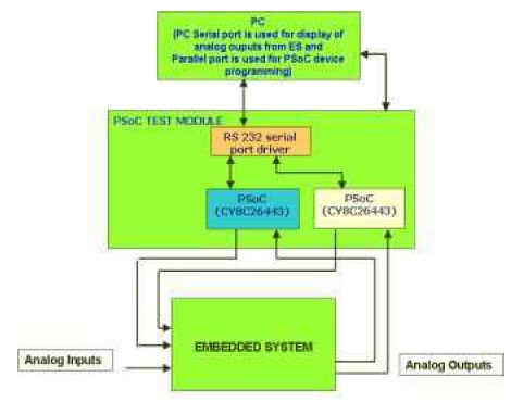
Figure 2. Block Diagram of Test Module
The test module has to generate the four analog outputs in the range 0 to 5 volts which are programmable. These outputs are given as inputs to ES. There are two PSoC devices used in the design, therefore each PSoC device produces two analog outputs (Millman & Halkais, n.d). Hence each PSoC device must have two Digital-to- Analog converters (DACs). Two 8-bit DACs are implemented on each PSoC device (Kane, 2012).
The test module has to capture the four analog outputs generated by ES and display them on serial port in hexadecimal format. Hence, there must be four Analogto- Digital converters (ADCs) on the test module. Since there are two PSoC devices in the design, two 12-bit ADCs are implemented on each PSoC device. Also two UARTs (Universal Asynchronous Receive Transmit) are implemented on each PSoC for serial communication. Two RS-232 communication ports (com1 & com2) on the PC are used for displaying on the serial window. Microsoft's hyper terminal is used as serial window. In addition, a 8-bit counter is implemented on each PSoC device to generate a clock required for UART to operate at 9600 baud rate, which is standard baud rate used in ES communication. Four unity gain amplifiers (Choudary & Jain, 2003) are implemented, two on each PSoC. The analog inputs to PSoC are routed through amplifiers. TTLto- RS 232 driver (Data sheets of MAX 233 Device) is used for serial communication. Both the channels contained in the device are used for com1 and com2. Pins are assigned for inputs to ADC, outputs from DAC and Tx & Rx lines of UART. All the required signals are brought out and terminated on 25 pin D-type connector from where the test module is connected to ES. The ADC and DAC implementation in PSoC devices is as shown in Figures 3 and 4, respectively.

Figure 3. ADC Implementation in PSoC Device
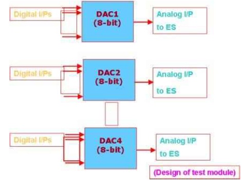
Figure 4. DAC Implementation in PSoC Device
The above hardware is configured using PSoC designer software IDE. The functionality of all peripherals placed on PSoC is programmed in C language. The implementation procedure is outlined below (Kanithkar, 2007).
STEP 1
Create a new Project in PSoC designer: In this we have to enter the name of the project and its location. Then we have to select the device family and part number then choose either 'C' or assembly as the program language.
STEP 2
Select User module selection view. In this we will see the various user modules that the user can select and place them on the PSoC device. It displays how many digital and analog blocks the user module will take and how much ROM and RAM the user module will take to place it on the PSoC.
STEP 3
Select Interconnect View. This is also known as device editor. Each user module will require one or two digital blocks and/or one or two analog blocks for its implementation. Here user has to decide on which of the digital and analog blocks the user module can be implemented. After choosing the blocks, the user can place the module (Albus, 2007). Then user has to select the user module parameters and global resources from the list of predefined parameters. Then the user has to assign pins for inputs and outputs. For assigning pins, the user has limited flexibility as the architecture is designed like that. Repeat step 3 for all the user modules that the user selected in step 2.
STEP 4
Then click “Generate Application” icon. This will create all the source code required for the device configuration.
STEP 5
Now enter “Application Editor ” session of IDE (Documentation of PSoC designer software IDE, Data sheets of CY8C26443 PSoC device). Under application editor window, we can see source files, library source files, and library header files corresponding to the user modules selected. There will be two source files: 'boot.asm' and 'main.c'. Now the user has to open the 'main.c' file and then write his code for the functionality of the PSoC, for example processing of data from user modules.
STEP 6
Now compile the 'main.c' file until no error occurs, then build the application, this will generate .rom file, which can be used for debugging or for programming the physical device.
STEP 7
Now enter “Debugger” session. The debugger session allows the designer to test the coded application in a physical system while providing an internal view of the PSoC device. Debugger commands allow the designer to read and write program and data memory, read and write I/O registers, read and write CPU registers, set and clear breakpoints, and provide program run, halt, and step control.
STEP 8
Programming the physical device. Click program part icon to program the device. Before doing that we need to connect the programmer (small hardware unit) to In Circuit Emulator (ICE) using a cat5 patch cable and place the device in programmer's socket. An external power is required to ICE. On clicking program part icon, the .rom file will be downloaded into the device is flash memory. A message would be displayed to that effect. Steps 1 to 8 have been done for programming the PSoC devices.
The developed Test Module is connected to ES. The test setup is shown in Figure 5. Individual power supplies are connected to ES and test module. Test module operates on 5 volts and ES requires 28 volts power supply. Both the test module and ES are connected to personal computers.
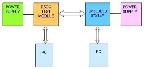
Figure 5. Test Set-up
Upon power ON to test module and ES, the embedded programs in test module and ES start executing. Actually there are two modes of operation in ES. One is called monitor mode and the other is called real mode. Testing of ES has to be done in both modes. In monitor mode, the ES can generate its commands (outputs) and accept inputs. This can be monitored from the PC connected to ES. In monitor mode, through PC connected to ES, commands can be generated and can accept the inputs and display them on PC. In real mode, the ES will be executing the real time code. In real time mode, the ES cannot be controlled through the PC connected to it. The ES operates in real time mode during the actual application. The test module software is written to provide a user interaction during testing. Using Test Module, we can perform testing of ES in both monitor mode and in real time mode (AN10E40datasheet). The tester can choose whether he wants to test analog inputs or outputs. Then accordingly, actions are to be performed on ES side, if it is in monitor mode. The test results can be observed on the PC connected to Test Module. With the above setup, analog I/Os testing of ES has been successfully carried out and the observations are in line with the expected values. After implementing the PSoC programming, the internal modules and their placements are as shown in Figure 6.
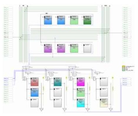
Figure 6. PSoC Architectural View After Programming
The final integrated test setup developed is tested for its functionality by giving the necessary voltages to the test setup. If the test is fault free, it is used for testing the ES. The role of ES is to perform the necessary operations with the input parameters generated from the DACs of PSoC and issue the output commands, which are observed on ADCs of PSoC. The outputs are observed on the PC monitor screen of Test Module. The results are as shown in Figures 7 and 8.
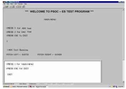
Figure 7. ADC Test Running
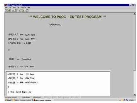
Figure 8. DAC Test Running
The test module designed using PSoC is very small in size and can be tailored to meet the complete testing of ES. This is in contrast to the earlier add-on card version of testing and was more general. As the test module consists of microcontroller based PSoC with on chip memory and peripherals, the testing is more matured and intelligent than earlier methods. There is flexibility in changing the types of ADCs, DACs, and their resolution that was not possible with the discrete ICs on the add-on card. The cost and development time of this test board is much less than the cost of add-on card. The dynamic reconfigurability of PSoC makes the user to use this device for many applications.