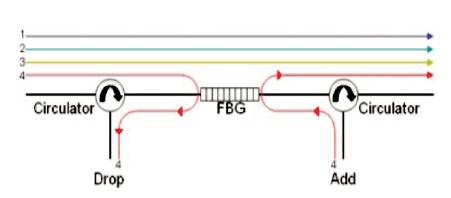
Figure 1. Optical Add-drop Multiplexer, using a Fiber Bragg Grating and Two Circulators [13]
The objective of this research paper is to study the band gap of different materials, so they can be used for designing of an efficient photonic crystal based add drop filter for an optical communication system. Today most of the transmission takes place in 1550 nm window, which is the most modern mode of communication. So a suitable material can help to enhance the overall system performance. The composition of gallium, indium, and phosphorus introduce the semiconductor material called GaInP. It is used in high-power and high-frequency electronics because of its superior electron velocity with respect to the more common semiconductors silicon and gallium arsenide, but in this case the Si is considered to be more promising than the GaInP due to the band gap structure which is analyzed by various simulations. A crystal is periodic arrangement of atoms and molecules and the pattern which the atoms and molecules are repeated in space is the crystal lattice. In the PhC the atoms or molecule are replaced by macroscopic media with differing dielectric constants and the periodic potential is replaced by a periodic dielectric function. The Wavelength Division Multiplexing (WDM) is considered to be a propitious scheme for high capacity optical interconnects and it is essential for designing of an optical filter. The FDTD and PWE methods are ideal for the structural analysis of an PhC structures, here in this paper the Rsoft and Lumerical softwares are used for carrying out required simulations.
Currently optical communication are one of the best solutions used in data transmission across very large distances while keeping high bit rates. In order to have full advantage of optical communication networks, a whole optical network is needed, which is composed of full optical devices, such as optical filters, optical demultiplexers, optical switches, etc.
Optical filters are essential and crucial passive components for modern optical communication systems. Microwave guide and fiber based ring resonator are also good due to their versatile functionalities and compactness. They can be designed for different By applications.
In wavelength-division multiplexing systems for multiplexing and routing different channels of light into or out of a Single Mode Fiber (SMF), an Optical Add-Drop Multiplexer (OADM) is used. Channel add-drop filter are critical component for WDM and have been previously demonstrated in microring resonators whose traveling wave mode structure enables complete sepration of input, drop and through ports without the need of optical circulators.
Extremely compact Photonic Crystal (PhC) based bandpass filter are attractive for their strong potential for large scale integration in Wavelength Division Multiplexing (WDM) communication networks. Many theoretical and experimental works have reported very promising results in particular with the realization of 4 channels WDM optical add-drop multiplexer (OADM), demonstrating its technology readiness level [7].
Artificial structures with periodic dielectric modulation, such as photonic crystals (PhC) can exhibit frequency ranges in which the propogation of electromagnetic waves is prohibited. This prohibition of wave propogation is tagged photonic band gaps (PBGs). These structures have many potential applications because of their ability to control light-wave propogation and to be integrated into optical circuits [2].
The transmission characteristics for single-ring and multiplering configurations can be encountered by using the twodimensional (2D) finite-difference time-domain (FDTD) technique in triangular lattice photonic crystal (PC) silicon rods. Both forward and backward dropping were achieved in dual-ring PCRR structures [5].
In this present work, a photonic crystal based add-drop filter is designed for optical communication system. First to analyze the bandgap of two suitable material which are GaInP and Si and second is to design the filter structure in the slab using defects. In this work line defects are used to create the waveguides in the slab.
The authors have chosen the holes in a slab phenomena as other phenomena in which rods in air cannot be realised in general. The design is based on cavities in a slab between two waveguides and the holes in the cavities are increased by 0.12 micrometers. The Gaussian source is applied at the input port, after the transmission it is analysed that the transmission spectrum lies in the third optical window with the approximate loss of 0.2 dB.
The implementation of the photonic crystal based filters in an optical device can improve the overall system functions and results in providing better efficiency for the optical communication devices. The slightest change in the photonic crystal can showcase significant changes in the optical communication system, so the designing can be easy as compared to other system modules. The designing process is comparatively easy as compared to the conventional filters like bandpass, bandstop, lowpass, and optical notch filers, so it will be beneficial to use optical filters in the communication devices.
Photonic crystal is a periodic crystal structure of dielectric characteristic or showing periodicity in a certain direction. When an electromagnetic (EM) wave propagates in a periodic structure whose period is equal to the wavelength of impulse, then it generates a Complete Photonic Band Gap (CPBG). Creation of new defects into the PC structure engenders that particular range of wavelength can be used as propagation region inside the structure.
These defects are mainly two types, first one is point defect or micro-cavity and the second one is line defect or waveguide. 2DPCs consist of dielectric rods in air host (high dielectric pillars implanted in a low dielectric medium) or air holes in a dielectric region (low dielectric rods in a higher dielectric lattice). There are lots of applications related to the photonic crystal ring resonators which may act as demultiplexers, band stop, and band pass filters. Due to the miniaturization, PCRRs are the most commonly needed filter used for the design of integrated optics.
In most of the designs PC structure consists of holes arranged in a hexagonal lattice on a silicon slab. The nanoring resonator is formed by removing certain holes along a hexagonal trace. The hexagonal nanoring resonator is sandwiched by two PC waveguides that are formed by removing two lines of holes [3].
An optical add-drop multiplexer (OADM) is a device used in wavelength-division multiplexing systems for multiplexing and routing different channels of light into or out of a Single Mode Fiber (SMF). This is a type of optical node, which is generally used for the formation and the construction of optical telecommunications networks. “Add” and “drop” here refer to the capability of the device to add one or more new wavelength channels to an existing multiwavelength WDM signal, and/or to drop (remove) one or more channels, passing those signals to another network path. An OADM may be considered to be a specific type of optical cross-connect. The optical add drop multiplexer can be of many types, Figure 1 shows a basic diagram of an Optical add-drop multiplexer using a fiber bragg grating and two circulators[13].
Figure 1. Optical Add-drop Multiplexer, using a Fiber Bragg Grating and Two Circulators [13]
An optical Add-Drop Filter (ADF) design is based on ultracompact Photonic Crystal Ring Resonators (PCRRs). the normalized transmission spectra for single-ring configurations have been investigated by using the twodimensional Finite Difference Time Domain (FDTD) technique in a square lattice dielectric-rod photoniccrystal structure. The introduction of four scatterers at the corners of quasi-square-ring PCRR, high wavelength selectivity, and close to 100% drop efficiency can be obtained [9].
An optical ring resonator is a set of wave-guides in which at least one is a closed loop coupled to some sort of light input and output. The basic structure of an optical ring resonator is depicted by Figure 2 [10].
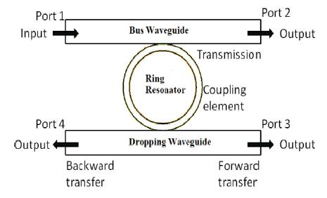
Figure 2. Basic Structure of Optical Ring Resonator [10]
Figure 2 shows the basic structure of an ring resonator. Optical ring resonators work on the principles behind total internal reflection, constructive interference, and optical coupling.
The Plane Wave Expansion (PWE) method and 2D Finite Difference Time Domain (FDTD) method are employed to obtain the Photonic Band Gap (PBG) range and output spectra of the ADF. Close to 100% of coupling and dropping efficiencies [11], the resonant wavelength tuning possibilities of ADF are theoretically studied to cover the lower channels of CWDM systems. The structural parameters, such as refractive index, lattice constant, and radius of the rod in the structure are considered for resonant wavelength tuning.
After designing the channel-drop lter, they investigated the effect of different parameters on the output wavelength of the lter. It has been shown that by changing the dielectric rods refractive index, radius of initial structure rods, and the radius of the 12-fold quasicrystal rods different output wavelengths of the filter can be obtained [6].
While doing the research the authors have seen many new design of Channel Drop Filters (CDFs) based on Photonic Crystals Ring Resonators (PCRRs). In some of the systems the filter characteristics for single-ring and dual-ring configurations based on two-dimensional (2D) triangular lattice Photonic Crystal (PC) silicon rods have been investigated by using the two-dimensional (2D) Finite- Difference Time-Domain (FDTD) method [12].
One of the filters design by the Finite-Difference Time- Domain (FDTD) algorithms were designed to work in 1552 nm, 1553 nm, 1554 nm, 1555 nm, 1556 nm, 1557 nm, and 1558 m with 1nm channel spacing and 0.2 m spectral line width, 96% to 100% transmission efficiency, and quality factor to be 8000, respectively. The results are discussed at the end for the use in Photonic Integrated Circuits [1].
Figure 3 shows the methodology for the system designing, which has been designed by these following steps.
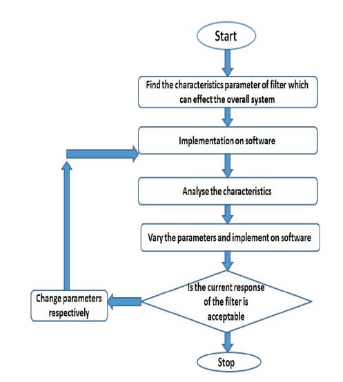
Figure 3. Flow Chart for System Design
The performance parameters are found for the system which can effect the overall system and the slightest change in them can modify the overall optical communication system.
In this work, two softwares are used for the implementation of add drop filter (photonic crystal based), first one is Rsoft for the analysis of the materials which can be used in the filter designing process and another is Lumerical for the main designing.
In this section the characteristics of that filter are analyzed and then find the areas which can be modified for a better output response are found.
After the successful implementation of the modified design, we can check whether the filter response is desirable or not.
The modelling and the designing of the system model is obtained by following two steps:
First to find a suitable material for the filter design the characteristics of Silicon and Gallium Indium Phosphide are analyzed using PWE (Plane Wave Expansion) method [4], as these these two materials show the existence of high Photonic Band Gap PBG.
In the Rsoft software BandSOLVE module is used for finding the band structure of the photonic crystal. A Band-SOLVE simulation can be started via either the Graphical User Interface (GUI) or a command line interface. The GUI operation of BandSOLVE is a very straightforward process.
To know the overall system model the photonic crystal and the suitable characteristics of an add drop filter which is to be used in a optical system for the filtering purpose and altering the waves in that particular system should be understood. Optical properties of photonic crystal are determined by the existence of the refractive index of the medium. The system model mainly consist of the following,
The various simulations are done with the help of Rsoft (Photonic Crystal Design Suite) software for a silicon and Gallium Indium Phosphide slab. The structure is designed with the same lattice constant a and the radius of the holes in a hexagonal (holes in a slab) structure, but after the simulation we can see the differences between the band gap.
Figure 4 shows the TE/TM band structure of the silicon slab, where the PBG band ranges between 0.26 to 0.33 and Figure 4 shows the TE/TM band structure of the slab, and the PBG band ranges for Gallium Indium Phosphide between 0.48 to 0.63. The Gallium Indium Phosphide has a very large band gap (1.89 eV), but silicon can provide a better optimization of PhC structures for the designing of optical components like add drop filters.
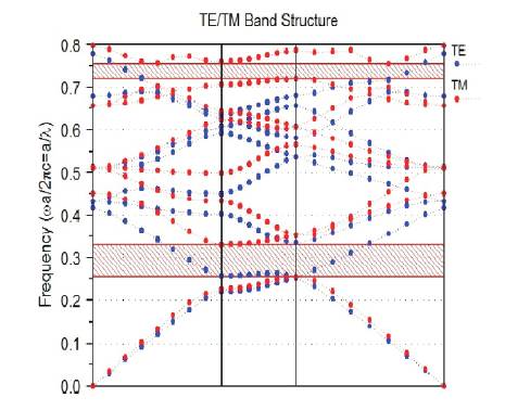
Figure 4. TE/TM Band Structure of Silicon Slab
The Figures 5 and 6 show the PBG structure of the both materials (Gallium Indium Phosphide and Silicon). The efficient transmission should be done in third communication window so the transmission can be less lossy, but the PBG band of Gallium Indium Phosphide ranges between 0.48 nm to 0.63 nm, which gives the wavelength of 850 nm to 650 nm, as it is known that the third window lies between 1530 to 1570 nm so the silicon can be a better material as compared to Gallium Indium Phosphide.
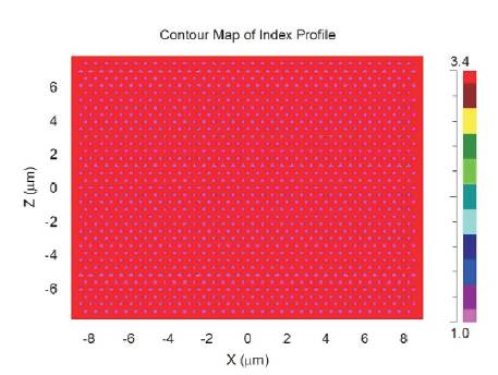
Figure 5. Material Fit Contour Map of Silicon Slab
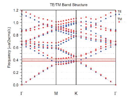
Figure 6. TE/TM Band Structure of GaInP Slab
The FDTD solutions are done by the Lumerical FDTD software. FDTD Solutions employs the industry proven Finite Difference Time-Domain (FDTD) method to accurately simulate optical and photonic devices involving wavelength scale structures. It can solve arbitrary geometries and materials, over any source bandwidth.
Figure 7 shows a photonic crystal based single ring hexagonal structure in the triangular lattice, where the lattice constant is set at 0.39 nm, while the radius is kept as 0.111 nm for the structure. The guassian source is applied at the input port and the transmission spectrum is analyzed at other three ports. The transmission of various ports for photonic crystal based single ring hexagonal structure in the triangular lattice is shown in Figure 8, where the highest peak for the transmission is occurred at the 1500 nm to 1550 nm, there can be various peaks, but the larger one is considered for the system module.
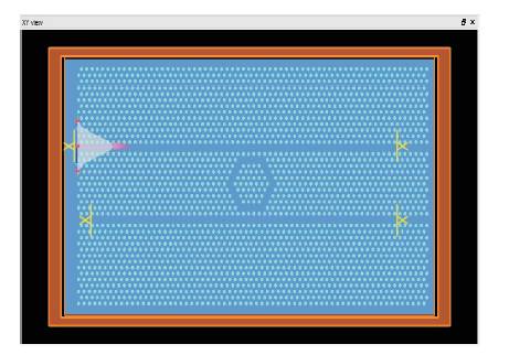
Figure 7. Silicon Based Single Ring Hexagonal Structure in Triangular Lattice
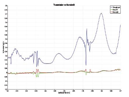
Figure 8. Transmission Spectrum of the Various Ports of a Single Hexagonal Ring Structure
Figure 9 shows the final filter structure designed in the software with FDTD module.
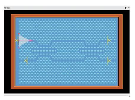
Figure 9. Modified Filters Layout in The FDTD Module
After simulating the filter structure by increasing the radius of the holes at the cavity, the filter transmission responds in the third window of the optical communication, with low drop efficiency and high Q factor. Figure 10 shows the transmission versus wavelength plot of the Through Port. The highest peak occurs between the 1564 nm to 1568 nm, which is actually quite ideal for the proposed design of photonic crystal based add drop filter which can show the results in the third window of the optical communication system with the least loss of 0.2 dB.
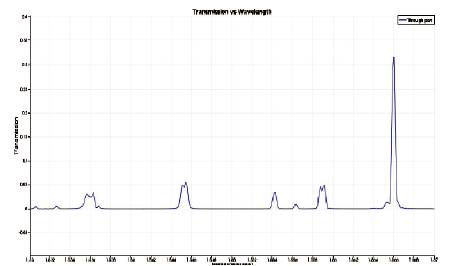
Figure 10. Transmission vs. Wavelength Plot of the Through Port
Figure 11 shows all the transmission results between the Through Port, Drop Port Left, and Drop Port Right. It can be seen that the transmission lies between the 1550 nm to 1570 nm, which is the third window of the optical communication with the least loss of 0.2 dB.
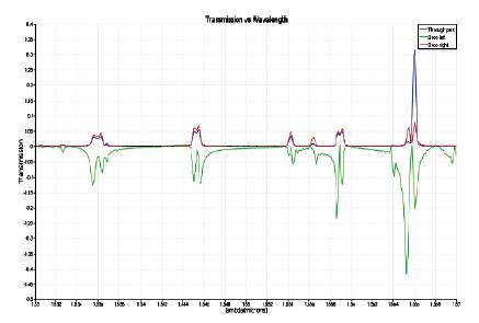
Figure 11. Transmission vs. Wavelength Plot of the Various Ports
The multichannel in the system can also be convenient instead of using particular number of channels. These kind of devices would be more useful for the realization of integrated optic circuits for CWDM systems and future access and metro networking applications.
The authors would like to acknowledge the Department of Electronics and Telecommunications Engineering of Shri Shankaracharya Technical Campus for providing the facilities to carry out this work and to the supervisors Mr. Vikas Sahu and Mr. Sharad Mohan Shrivastava for their guidance and cooperation throughout the whole paperwork.