
Figure 1. ADS Layout of Microstrip Patch Antenna
In this paper, a new technique is proposed to achieve size reduction of microstrip patch antenna using Defected ground microstrip patch antenna. The technique is based on etching out two rectangular slots from the metallic ground plane beneath the complementary of the patch antenna. To achieve circular polarization a probe feed with different axial ratio has been proposed. Due to unequal axial ratio of 1:2 asymmetry is introduced. The slot length is used to optimize the resonant frequency. The validity of the concept is demonstrated by considering two resonance frequencies which are obtained at 2.4 GHz and 2 GHz. The proposed antenna dimension is 40x70 mm2 . The dielectric substrate FR4_epoxy of relative permittivity 4.4 and dielectric loss tangent 0.02 is used for simulating the results. The simulation is done on Advanced Design System (ADS) version 11.
Circularly Polarized (CP) microstrip patch antenna has advantages over microstrip patch antenna because it combines the characteristic of both the microsrtip patch antenna and circularly polarized patch antenna [1]. Over the past decade microstrip patch antenna has got a lot of acceptance due to its properties like light weight, low cost, low profile planar configuration and compatibility with monolithic microwave integrated circuit (MMIC).After the invention of microstrip patch antenna, a lot of research and development activity has been carried out to meet the modern requirement of compact wireless communication devices by improving the impedance and radiation pattern of the concerned microstrip patch antenna. From the inception, the downscaling and compactness of radiating elements becomes very important in wireless communication devices. Apart from these entire advantages, microstrip patch antenna suffers from narrow impedance bandwidth. To improve this obstacle, stacked microstrip patch antenna or U and Eslot- loaded patches of coupled resonator structures are used [2]-[3]. The VSWR impedance bandwidth of E-shape and U-slot-loaded single-layer rectangular microstrip patch antenna are 30%-35% on electrically thick substrate material [2]-[5]. Apart from this , if a foam substrate is used in dual U-slot-loaded microstrip patch antenna, then impedance bandwidth of approximately 44% is obtained.
Apart from defected ground structure, to reduce the size of antenna, dielectric material with high-permittivity is used. But this method is not very appropriate as it deteriorates the far-field performance of the antenna due to creation of surface waves. Various techniques have been suggested in the literature for size reduction in microstrip patch antenna .Material having ceramic substrates were used in size reduction of microstrip patch antenna [6]. Other methods for size reduction include artificial magnetodielectric surfaces, and high impedance surface (also known as meta-surfaces) [7]-[9].
Recently, metamaterial having the characteristic likes double-negative material and artificial magnetic material in the form of Split-Ring Resonator (SRR) have been used for the size reduction [10]. For the first time, Falcone et al proposed the complementary split-ring resonator (CSRR) as dual counterpart SRRs [11]. The proposed resonator has been widely studied, synthesized and applied in the design of the filters and microwave circuits [12]-[13]. The difference between the two structures were based on the excitation method. The SRR unit cell responds to an axial magnetic field but the CSRR resonates upon excitation of an axial electric field. Due to these advantages the equivalent circuit of CSRR can be drawn in the form of an LC resonator tank circuit, neglecting the metallic and dielectric losses.
From the invention of CSRRs, the potential application of CSRRs have been explored in the size reduction of patch antenna [14]-[16]. It is important to mention that microstrip patch antenna have been relieved of loading with CSRRs, while other methods for size reduction include the etching out the CSRRs randomly from etching metallic ground plane. Using these types of methods would increase design complexity and also difficulties will be felt while finding the exact location for CSRRs beneath the radiating patch antenna.
In this work, authors demonstrate through numerical simulation the etching of the ground with two rectangular slots of unequal lengths. The design was simulated using Agilent Advanced Design System version 11. The results are very encouraging as it reduces the size of the microstrip.
The structural organization of the paper is as follows. In Section 1 objective of the paper is given, Section 2 explains the methodology used in this paper. In Section 3 the geometry of antenna is discussed. Section 4 deals with the simulated impedance matching of the proposed antenna. Finally conclusion is presented. Further simulation results were carried out using Finite-Element Method (FEM) based program Agilent Advanced Design System version 11.
The objectives of this paper are to reduce the size of the microstrip patch antenna by defected ground structure and to introduce the asymmetry in the structure to make the antenna circularly polarized by changing the axial ratio of the given antenna.
Initially successive approximation method has been used to find out the minimum size of the radiating patch antenna. The result of the minimum size antenna has been shown in Figure 3. To reduce the size of microstrip patch antenna various methods had been proposed. These methods include the uses of foam substrate and using a material of high dielectric constant. Apart from these conventional methods Split-ring resonators (SRR) and complementary split-ring resonator (CSRR) had also been used. In this paper, a method based on complementary rectangular slot on the ground plane of the radiating patch antenna has been proposed. This complementary rectangular slot has been introduced just beneath the radiating patch antenna. Due to this asymmetry the sizes of the proposed antenna reduces, and result of the reduced size structure shown in Figure 4.
The geometry of E shape patch on a FR4 epoxy (Ɛr =4.4 and tan ξ = 0.02 of thickness, h = 1.6 mm is shown in Figure1. A 50Ω coaxial SMA probe feed connector is used for feeding the patch antenna. A dielectric substrate on the top of ground has been used for antenna fabrication, which requires soldering of SMA connector on the patch. The original length and width of the patch antenna is 40x70 mm2 in which some modification has been done. These modifications include two slots of length 7x15 mm2 and 7x30 mm2 on the radiating patch. Also complementary to the radiating patch in the ground plane rectangular slots of length 7x25 mm2 and 7x10 mm2 had been etched . All these proposed modifications are part of the E shape antenna. The dimension of antenna is shown in Figure 2. The dimension of finite ground in the proposed antenna is same as the dimension of the patch (also 40x70 mm2 ).
These lengths are taken after performing some initial experiment on the dimension of the ground plane. These results are based on Finite-Element-Method (FEM) based program Advanced Design System (ADS) version 11.
Figure 1. ADS Layout of Microstrip Patch Antenna
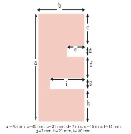
Figure 2. Dimensions of the Proposed Microstrip Patch Antenna
The antenna was initially constructed on E shape for a resonant frequency of 2.4 GHz [1]. The features of finite structures of Advanced Design System are used for subsequent simulation of the antenna. The simulated result is shown in Figure 3.

Figure 3. Simulated Return Loss of Antenna without Defected Ground Structure
In current time, discontinuities are introduced in ground plane or in microstrip lines to improve the performance of different passive circuits. Due to these discontinuities size reduction of amplifier, the enhancement of filter characteristics [17]-[18] and harmonic are suppressed in patch antenna. Also, for the size reduction, a new proposal called defected microstrip structure (DMS) [19] has been successfully used. This technique can also be used in tuning technique for rectangular patch antenna. There are lot of similarities between the structure (called spurline and defected microstrip structure (DMS)).
The spurline is a type of radio frequency and microwave distributed element filter with band-stop (notch) characteristics, most commonly used with microstrip transmission lines. Spurline usually exhibit moderate to narrow-band rejection, at about 10% around central frequency. Both are etched in the microstrip line and behave as stop-band filters [20]-[21]. However defected microstrip structure (DMS) has achieved a greater associated inductance in comparison to the spurline. It exhibits a greater slow–wave effect, and it will provide a longer trajectory to the electromagnetic wave. Due to more discontinuities present in the DMS. Also, compared to the spurline, DMS performs a greater stop-band bandwidth inspite of both having the same dimension. DMS are used in the transmission line to increase in the slow-wave factor (SWF) for the size reduction of passive planar circuits like microstrip line lengths, coupling lines and microstrip antenna, where the defected ground structure is used. However, as to how this phenomenon happens, no mathematical method has been explained so far.
In conclusion, to reduce the size of microstrip patch antenna a technique is presented. This proposed technique is based on introduction of complementary rectangular slot on the ground plane just beneath the radiating patch antenna. Also by changing the axial ratio of radiating patch antenna it can be made to polarize circularly. In this paper, microstrip patch antenna was designed using conventional methods for operating at 2.49 GHz frequency and another antenna was designed using defected ground structure. The defected ground antenna shows a resonating frequency of 2 GHz. The result of the defected ground structure is shown in Figure 4. Thus we are able to reduce the size of the microstrip patch antenna. The advantages of a smaller area are that we can reduce the cost and also that we can even pack more antennas into the system.
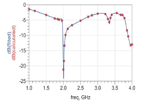
Figure 4. Simulated Returns Loss of Antenna with Defected Ground Structure