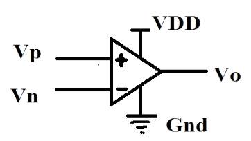
Figure 1. Comparator
The main building block of any portable electronic equipment is the Analog-to-Digital Converter. The increased demand of the portable electronic equipments has forced the circuit designers to use lower supply voltages. However, the performance of analog circuits is degraded at low supply voltage due to large power dissipation and higher noise occurrence. This makes the design of voltage analogue circuits more challenging. As comparator is the basic device of analog to digital converters, this paper aims to analyze the comparator design with hysteresis. This proposed technique reduces the power dissipation and noise. The results were compared with the double tail comparator, which operates with supply voltage of 0.6v.
Comparator is a basic device in analog to digital converters. Now-a- days, many high speed analog to digital converters are required with low power. The designing of high speed comparator is difficult when the supply voltage is small. In low voltage operation, common input range is important in many high speed ADC architectures, like flash ADC. For this kind of low power comparators, many techniques were followed in previous methodologies, such as supply boosting method [2], body driven technique [3] and latch type comparator techniques [4].
Body driven technique is used to achieve low voltage design. By using this method, the 1bit quantizer for Δmodulator [8] is proposed. Boosting and bootstrapping techniques are effective techniques, which are based on input supply, clock voltage and switching problems. An [5], [6], additional circuit is added to the existing conventional comparators for the purpose of increasing the speed of the comparator. Developing new circuit structure which avoids stacking too many transistors for low power operation, particularly do not increase the complexity of the circuit.
In the existing methods for low power application, double tail dynamic comparator is used. In this methodology the author has added additional circuit with the conventional dynamic comparator. This paper describes about another type of comparator called Hysteresis Comparator. This provides high speed operation and low power dissipation when compared to the previous double tail dynamic comparator.
Comparator is a circuit that compares an analog signal with another analog signal or reference and outputs a binary signal based on the comparison as shown in figure 1. If the +, Vp, the input of the comparator is at a greater potential than the -, Vn, input, the output of the comparator is a logic 1, where as if the + input is at a potential less than the – input, the output of the comparator is at logic 0.
Vp < Vn, then Vo = Gnd= logic 0.
Vp >Vn, then Vo = VDD= logic 1.
In previous days, clocked comparators were chosen for the high speed analog to digital converters applications. But now-a-days many methodologies are presented to overcome the problem of clocked comparator, like speed [5], [6], noise [7], low supply voltage [2].
Figure 1. Comparator
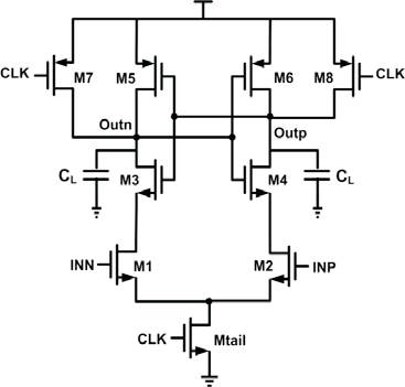
Figure 2. Conventional Comparator
Figure 2 is a conventional comparator [1], in analog to digital converters, which is widely used. Generally, comparator operates in two phases called reset phase and decision making phase (or comparison phase). In reset phase, clk=0 and Mtail is OFF. Transistors M7 & M8 pull and the output nodes Outn and Outp to Vdd. In comparison phase, clk=Vdd. Transistors M7 & M8 both are OFF, and Mtail is ON. Output voltages (Outp, Outn), which had been pre-charged to VDD, Node INN & INP start discharging with different phases. Assuming the case where VINP > VINN, Outp discharges faster than Outn, Outn pulls to VDD and Outp discharges to ground. If VINP < VINN, the circuits continuously operate in this conditions.
The disadvantage of this comparator is that it needs several stacked transistors, and a sufficiently high supply voltage is needed for a proper delay time. Another one disadvantage is that there is only one current path, via tail transistor Mtail, which defines the current for both the differential amplifier and the latch.
Due to better performance of double-tail architecture in low-voltage applications, the double tail dynamic comparator is designed.
The circuit of a double tail dynamic comparator is shown in the Figure 3. It is an advanced methodology of the conventional comparator. This comparator also operates in both reset and comparison phase.
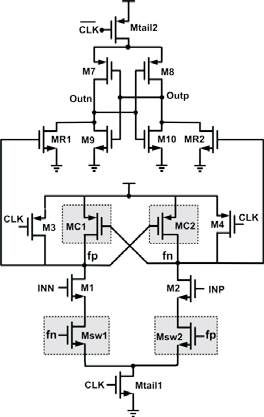
Figure 3. Double Tail Dynamic Comparator
In reset phase, clock is 0, Mtail1 and Mtail2 both are in OFF condition. M3 and M4 pull fn and fp nodes to VDD. At that time, the transistors MC1 and MC2 are cut off. The transistors MR1 and MR2 output to ground.
In decision making phase (comparison phase) clock = Vdd, Mtail1 and Mtail2 both are in ON condition. Transistor’s M3 and M4 are turn OFF. At the beginning of this phase, the control transistors are OFF. fn and fp start to drop according to various input voltages.
These dynamic comparators also suffer from large power dissipation, large area and noise. To recover from this problem, the author is using Hysteresis technique in comparators. By using this the comparator’s experimental result is to compare offset values, power dissipation, and speed of different structures.
The circuit of hysteresis comparator is shown Figure 8. When a positive feedback is appled the to the Schmitt trigger, it will act as a Hysteresis Comparator.
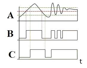
Figure 4. Outputs of a Schmidt trigger (C), Comparator Output (B), when a noisy signal (A) is applied.
In Figure 4, the green dotted lines are the circuit's switching thresholds. The Schmitt trigger tends to remove noise from the signal.
Noise is a random fluctuation in an electrical signal, and it is generated by electronic devices that vary greatly, as it can be produced by several different effects. Thermal noise is unavoidable at non-zero temperature, while other types of noises depend mostly on the device type or manufacturing quality and semiconductor defects, such as conductance fluctuations, including 1/f noise.
The solution for a noisy input is to use a comparator to apply the input voltage to inverting input. Because the positive feedback voltage improves the input voltage. A comparator using positive feedback is called Schmitt trigger. When the comparator is positively saturated, a positive voltage is the feedback to the non-inverting input. This positive feedback voltage holds the output in the high state. Similarly, when the output voltage is negatively saturated, a negative voltage is the feedback to the noninverting input, holding the output in the low state.
When the output is positively saturated, the reference voltage applied to the non-inverting input is

When the output is negatively saturated, the reference voltage is

In the inverting version, the attenuation and summation are separated. The two resistors R1 and R2 act only as a "pure" attenuators (voltage divider) as shown in Figure 5. The input loop acts as a simple series voltage summer that adds a part of the output voltage in series to the circuit input voltage. This series of positive feedback creates the needed hysteresis that is controlled by the proportion between the resistances of R1 and the whole resistance (R1 and R2). The effective voltage applied to the op-amp input is floating; so, the op-amp must have a differential input.
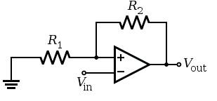
Figure 5. Schmitt trigger act as an inverting comparator
The circuit is named inverting since the output voltage always has an opposite sign to the input voltage when it is out of the hysteresis cycle (when the input voltage is above the high threshold or below the low threshold). However, if the input voltage is within the hysteresis cycle (between the high and low thresholds), the circuit can be inverting as well as non-inverting. The output voltage is undefined; it depends on the last state and the circuit behaves as an elementary latch.
To compare the two versions, the circuit operation will be considered at the same conditions as above. If the Schmitt trigger is currently in the high state, the output will be at the positive power supply rail (+VS). The output voltage V+ of the voltage divider is:
The comparator will switch when Vin = V+. So Vin must
exceed above this voltage to get the output to switch.
Once the comparator output has switched to −VS, the
threshold becomes
 to switch back to high. So this
circuit creates a switching band centered on zero, with
trigger levels
to switch back to high. So this
circuit creates a switching band centered on zero, with
trigger levels  (it can be shifted to the left or to the right by connecting R1 to bias voltage). The input voltage
must rise above the top of the band, and then below the
bottom of the band, for the output to switch off (minus) and
then ‘on’ back (plus). If R1 is infinity or R2is zero (i.e., a short
circuit), the band collapses to zero width, and it behaves as
a standard comparator.
(it can be shifted to the left or to the right by connecting R1 to bias voltage). The input voltage
must rise above the top of the band, and then below the
bottom of the band, for the output to switch off (minus) and
then ‘on’ back (plus). If R1 is infinity or R2is zero (i.e., a short
circuit), the band collapses to zero width, and it behaves as
a standard comparator.
This circuit does not have impact on the input source since the source is separated from the voltage divider output by the high op-amp input differential impedance.
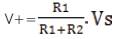
As shown in Figure 6, the two resistors R1 and R2 form a parallel voltage summer. It adds a part of the output voltage to the input voltage thus "helping" it during and after switching that occurs when the resulting voltage is near to the ground. This parallel positive feedback creates the needed hysteresis that is controlled by the proportion between the resistances of R1 and R2. The output of the parallel voltage summer is single-ended (it produces voltage in respect to ground); so, the circuit does not need an amplifier with a differential input. Since conventional opamps have a differential input, the inverting input is grounded to make the reference point zero volts.
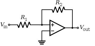
Figure 6. Schmitt trigger act as a Non inverting comparator
The output voltage always has the same sign as the opamp input voltage, but it not always has the same sign as the circuit input voltage (the signs of the two input voltages can differ). When the circuit input voltage is above the high or below the low threshold, the output voltage has the same sign as the circuit input voltage (the circuit is noninverting) as shown in Figure 7. It acts like a comparator that switches at a different point, depending on whether the output of the comparator is high or low. When the circuit input voltage is between the thresholds, the output voltage is undefined; it depends on the last state.
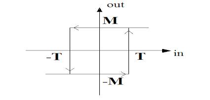
Figure 7. Non Inverting Comparator
For instance, if the Schmitt trigger is currently in the high state, the output will be at the positive power supply rail (+VS). The output voltage V+ of the resistive summer can be found by applying the superposition theorem:
The comparator will switch when V+=0. Then R2.Vin = -
R1.Vs(the same result can be obtained by applying the
current conservation principle). So, Vin must drop below  to get the output to switch. Once the comparator
output has switched to −VS, the threshold becomes
to get the output to switch. Once the comparator
output has switched to −VS, the threshold becomes  for Vs to switch back to high. So this circuit creates a
switching band centered on zero, with trigger levels Vs
for Vs to switch back to high. So this circuit creates a
switching band centered on zero, with trigger levels Vs  (it can be shifted to the left or the right by applying a
bias voltage to the inverting input). The input voltage must
rise above the top of the band, and then below the bottom
of the band, for the output to switch on (plus) and then back
off (minus). If R1 is zero or R2 is infinity (i.e., an open circuit),
the band collapses to zero width, and it behaves as a
standard comparator. The value of the threshold T is
(it can be shifted to the left or the right by applying a
bias voltage to the inverting input). The input voltage must
rise above the top of the band, and then below the bottom
of the band, for the output to switch on (plus) and then back
off (minus). If R1 is zero or R2 is infinity (i.e., an open circuit),
the band collapses to zero width, and it behaves as a
standard comparator. The value of the threshold T is  given and the maximum value of the output M is the power supply rail.
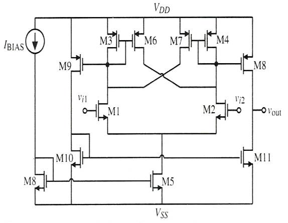
Figure 8. Comparator with Hysteresis
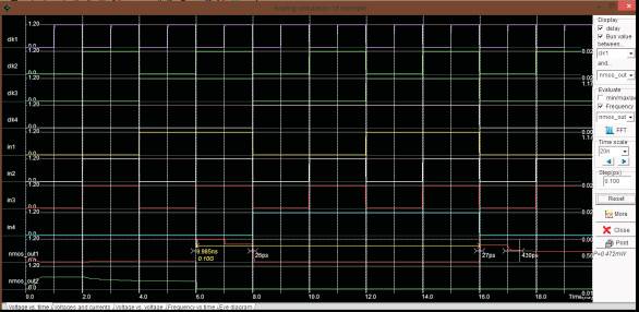
Figure 9. Simulation Result of double tail comparator (V vs T)
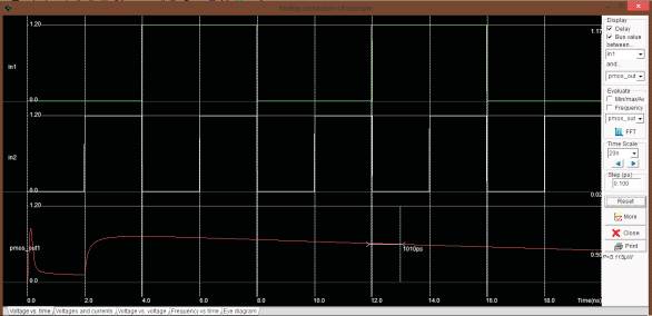
Figure10. Simulation Result of hysteresis comparator (V vs T)
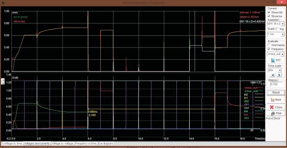
Figure 11. Simulation Result of double tail comparator (V vs I)
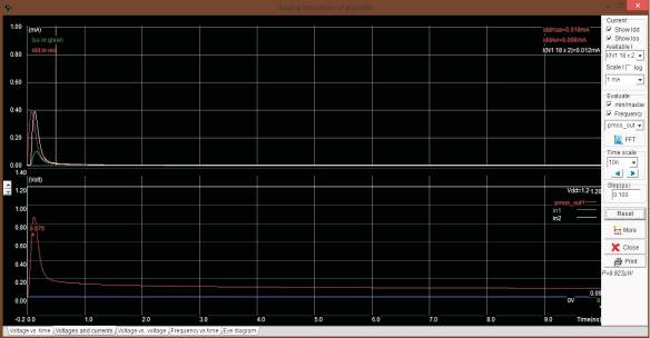
Figure 12. Simulation Result of double tail comparator (V vs I)
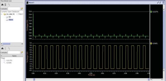
Figure 13. Simulation Result of double tail comparator for Noise
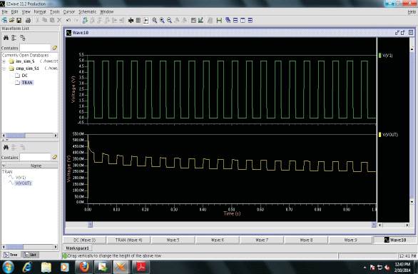
Figure 14. Simulation Result of hysteresis comparator for Noise
In order, the proposed comparator is simulated in all circuits at 9.923μW with the input voltage 0.6V compared with conventional dynamic comparator and double tail dynamic comparator.
Thus the simulation and analysis results for the double tail and hysteresis comparator shows that the power consumed for double tail comparator is 0.5 mW and for the hysteresis 5μW, as shown in Figures 9, 10, 11 and 12. These Figures show the simulation results of both double tail comparator and hysteresis comparator with respect to voltage and time, and voltage versus current, respectively. Figures 13 and 14, show the noise comparison of both double tail comparator and hysteresis comparator. This clearly shows that the proposed hysteresis comparator consumes fewer amounts of power and noise when compared to the double tail comparator from the simulation results.
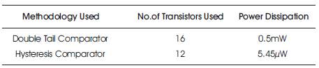
Table 1. Comparison Results
Table 1 shows the difference between the existing double tail comparator and the proposed hysteresis comparator.
In this paper, two common structures of double tail dynamic comparator and hysteresis comparators are analyzed. From the simulation results, it is evident that the proposed hysteresis comparator provides better performance than existing double tail dynamic comparator. New comparator consumes low power (5.45μW) when compared with double tail dynamic comparator (0.5mW) and Noise.