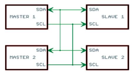
Figure 1. I/O Diagram of I2C Multi Master and Multi Slave Bus Controller
I2C Multi Master with Multi Slave is designed from a bidirectional serial data bus containing bidirectional data lines like Serial Data Line (SDL) and Serial Clock Line (SCL) along with Wishbone Signal. I2C protocol has the ability to support multiple masters and provides an efficient method of data exchange between devices. This is a very useful protocol for faster devices to communicate each other with slower devices without data loss. With the use of this protocol, a serious problem arises resulting to overlapping of signals. To overcome such problems, a special signal called WishBone signal is used. The main objective of this paper is to observe the operation of the master controller and wishbone controller, which performs high speed data transfer in the presence of master or slave. This yields higher speed data transfer over the network. The complete module is modeled in Verilog HDL and synthesized in Xilinx 13.2i, also simulated in Model Sim 6.4a.
In the world of serial data communication [2], I2C (Inter Integrated Circuit) bus has become a de-facto standard for short-distance communication among ICs. The I2C [1] bus uses two bi-directional open-drain wires with pull-up resistors. There is no strict baud rate requirement as with other communication standards like RS-232. The true multi master bus allows protection of data corruption if multiple masters initiate data transfer at same time. Many other features of the I2C bus provide efficient and flexible means for control functions that do not require high speed data transfer, and for applications that require a small amount of data exchange. The Wishbone bus interface is a free, open-source standard in digital systems that require usage of IP cores. This bus interfaces the reused IP by defining a common interface among IP cores and which provides portability for the system.
In this project, the implementation of Multi Master and Multi Slave I2C bus protocol with Wishbone signal for interfacing low speed peripheral devices on FPGA can be possible. It is also the best bus for the control applications, where devices may have to be added or removed from the system. I2C protocol can also be used for communication between multiple circuit boards equipped with or without using a shielded cable depending on the distance and speed of data transfer. I2C bus is a medium for communication, where master controller [6] is used to send and receive data between the master and the slave. The low speed peripheral is interfaced with I2C master bus [4]. Figure 1 shows the I2C bus system with Multi Master and Multi Slave. When using multi master arbitration, clock stretching needs to considered. Arbitration decides which master is going to rule the bus.
Figure 1. I/O Diagram of I2C Multi Master and Multi Slave Bus Controller
This paper is divided into following sections. Section 1 describes about the I2C protocol of the proposed design, which also presents the module description for the proposed system. Section 2 presents the software implementation along with algorithm and flowchart. Section 3 explains the simulated results using SPARTAN-3A. Section 4 describes the observation and finally the paper is concluded.
The I2C bus is a multi-master bus that supports a Multi- Master mode which allows more than one device capable of controlling the bus that is connected to it. Each I2C device is recognized by a unique address and can operate as either transmitter or receiver depending on the function of the device. In addition to being a transmitter or receiver, devices connected to the I2C bus can also be considered as master or slave when performing data transfers. A master device is the device that initiates a data transfer on the bus and generates the clock signals to permit that transfer. During this transfer, any device addressed by this master is considered as a slave.
When the master (controller) wishes to transmit data to a slave, it begins by issuing a start sequence on the I2C bus, which is a high to low transition on the SDA line, while the SCL line is high as shown in Figure 2 (a). The bus is considered to be busy after the START condition.
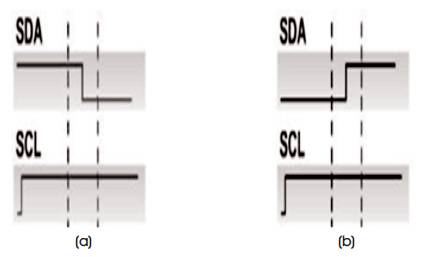
Figure 2 (a). “START” Sequence, (b) “STOP” Sequence
Figure 2 (b) shows the STOP sequence, where the SDA line is driven low while SCL line is high. This signal ends the transaction with the slave device.
The design has four main modules as depicted in Figure 3. This includes one top-level module and three lower-level modules, the byte command module and a bit command module [5].
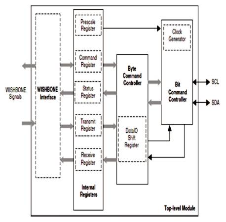
Figure 3. Block Diagram of I2C Module
In addition to connecting all the functional blocks together, this module generates byte-wide data, acknowledgement, and interrupt for the Wishbone interface.
I2C bus has only two wires which are SDA (Serial Data Line) and SCL (Serial Clock Line). SCL acts as a clock line for I2C bus, where SDA acts as a data line. The SCL and SDA lines are connected to all devices on the I2C bus. As both SCL and SDA lines are “open drain” sources [11], the I2C bus is said to be idle when both SCL and SDA are at logic 1 level.Depending on the parameter ARST_LVL, the reset polarity is determined and distributed to all the modules.
The microcontroller issues commands and data through the Wishbone interface in byte format. The information is fed into the byte command, controller module and is translated into I2C sequences required for a byte transfer [3]. This module includes a state machine as shown in Figure 4 to handle normal I2C transfer sequences.
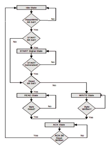
Figure 4. I2C Byte Command Finite Machine
Bit command controller module directly controls the I2C bus, SCL and SDA lines, by generating the correct sequences for START, STOP, Repeated START, READ, and WRITE commands. Each bit operation is divided into five (5 x SCL frequency) clock cycles (idle, A, B, C, and D), except for the START command that has six clock cycles. This ensures that the logical relationship between the SCL and SDA lines meets the I2C requirement for these critical commands [10]. The internal clock running at 5 x SCL frequencies is used for the registers in this module.
By the nature of open-drain signal, the I2C provides clock synchronization through a wired-AND connection on the SCL line. This clock synchronization capability can be used as a handshake between the slave and master I2C devices [8]. By holding the SCL line low, the slave device tells the master to slow down the data transfer until the slave device is ready. This design detects the SCL line to determine if the line is being held.
I2C bus is a medium for communication, where master controller is used to send or receive data to and from slave. I2C multi master with multi slave is designed using Verilog HDL [7] based on Finite State Machine (FSM). There are several states in obtaining the result.
1) IDLE: When SDA and SCL are HIGH, it will stay in idle state and will not perform any operation.
2) START: When SDA changes from HIGH to LOW and SCL is HIGH, then the I2C Master will start transmitting the signals.
3) WRITE: Master will send 8 bits of data from those 8 bits, in th that 7 bits are for address and 8 bit will be zero as it is a read operation.
4) If the address sent by Master is matched with Slave address, then Slave will generate positive acknowledge (ACK) pulse to the Master.
5) After reception of ACK, pulse Master will send 8 bit register address [12] to the Slave. Again if it is matched, then Slave will again generate ACK pulse.
6) Now DATA which needs to be written will be sent by the master in a packet of 8 bits. After reception of each packet, the slave sends ACK.
7) STOP: Once data transmission is over, Master will generate it by transmitting SDA from LOW to HIGH, when SCL is HIGH.
8) If I2C wants to perform READ operation, then it will also first go for WRITE operation and once the register is selected, after generating repeated START, it will go into READ operation. For that 8th bit of first data byte will be one.
9) Master will send slave address for read operation to the slave.
10) Master will receive data from slave and acknowledges the slave.
11) Master will generate STOP condition for termination.
This is the algorithm for the Master operation.
The flowchart describes the conversion of bytes into bits, which is transmitted by the Master to the Wishbone to avoid overlapping.
The I2C master with Wishbone interface design is simulated using an I2C slave model (i2c_slave_model.v) and a Wishbone master model (wb_master_model.v). The slave model emulates the responses of an I2C slave device by sending ACK, when the address is matching and when the WRITE operation is completed. The Master model contains several tasks to emulate WISHBONE READ, WRITE, and compare commands normally issued by the microcontroller. The top-level test- bench (tst_bench_top.v) controls the flow of I2C operations. The START, WRITE, REPEATED START, READ, consecutive READ, ACK/NACK, STOP, and clock stretching operations are simulated with the test bench.
The following timing diagrams show the major timing milestones in the simulation. Figure 5 (a) shows the simulation when the I2C Master READ enable is HIGH, this means it is ready to read the data from the slave. Figure 5 (b) shows that the Master is transmitting the data to the Slave when WRITE enable is HIGH. Figure 5 (c) and Figure 5 (d) show the I2C Master with Wishbone signal and Slave operations.
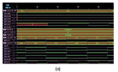
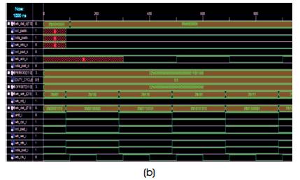
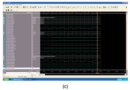
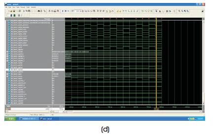
Figure 5 (a) I2C Master with READ Enable, (b) I2C Master with WRITE Enable, (c) I2C Master with Wishbone Signal, (d) I2C Master with Wishbone Signal and Slave Operation
This design is implemented in Verilog. When using this design in a different device, density, speed, or grade, performance and utilization may vary. Default settings are used during the fitting of the design.
The Performance and resource utilization of devices are illustrated in Table 1.
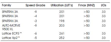
Table 1. Performance and Resource Utilization
From Table1, it is clear that SPARTAN 3A [9] with speed grade -3 is utilizing the less number of LUT's when compared with the other SPARTAN 3A [10] families and LATTICE families, but all the families are operated with the same frequency and the number of inputs/outputs is equal.
Hence, it can be said that by using SPARTAN-3A, the size of the device will be decreased and with this the speed of the device is increased.
I2C Multi Master Controller with WISHBONE interface is designed and implemented, and this method increases the performance of the design due to Multi number of masters and slaves that are connected to the WISHBONE interface. This method has reduced the overlapping of signals, which are transmitted by the master to the slave through WISHBONE Interface. Hence, by using this method, the overall performance of the device is increased, the transmission time decreases with the use of WISHBONE signal, overlapping of signal while using the Multi Master has overcome and the area is reduced. The future scope of this paper is “to extend the same with the Spartan3 FPGA [2] for knowing the worst path timing delay and its power constraints”.