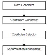
Figure 1. Flow diagram representation of RRC filter
FIR filters are widely used in wireless mobile communication systems such as channel equalization, matched filtering, and pulse shaping, due to their stability and reconfigurability. In this paper, the pulse shaping FIR filter such as root-raised cosine filter is designed for multistandard digital up converter. The two bit binary common sub-expression based binary common sub-expression elimination algorithm is used to ignore the occurrences in identical bit pattern. The number of additions and multiplications are reduced using this technique. Carry save adder is used to generate the partial product which reduces the area and increases the speed. The area and speed of the filter design is synthesized and simulated using Xilinx ISE 12.1.
Software Defined Radio (SDR) technology is widely used in wireless communication that replaces the analog signal processing in transceivers with digital signal processing to provide flexibility through reconfiguration. The SDR receiver uses channelizer with different communication standards. Effective reconfigurable Wireless Code Division Multiple Access Digital Up Converter (WCDMA DUC) design has been presented for mobile communication base stations. The different sections of Digital Up Converter (DUC) have been optimized separately and then combined together.
Ankita Mandal [1] had reviewed the reconfigurable FIR Filter architectures for low power by analyzing various methods. Common Sub-expression Elimination (CSE) method was used to reduce the adder operation, but it limits the filter coefficients. It has the possible of increasing the number of registers that increase the overall area consumption. Then Canonic Signed digit (CSD) was reviewed where minimum numbers of adders are used, but it is not suited for reconfigurability. Constant Shift Method (CSM) had been reviewed where the multiplication operation was performed by constant shifts. The power consumed is more and speed of the operation is increased. Programmable Shift method was analyzed where delay can occur that reduced the speed of the operation.
Anshika Rajolia, [2], analyzed the design of higher order Finite Impulse Response (FIR) Filter based on Canonic Signed Digit (CSD) to minimize the power consumption and increase the speed of operation. For this, Binary Common Sub-expression Elimination (BCSE) algorithm was presented by combining CSD and Radix4 CSD as arithmetic codes for channelizers. It provides better performance in terms of power and speed. It was overcome by conventional FIR filter methods based on the number of full adders used for coefficient multipliers.
Baha Ali Nasir et al. [3], designed the MAC FIR filter architecture for SDR system to reduce the multiplication operation and make the area efficient. For this, FIR filter using polyphase multiply accumulate (MAC) is used to decrease the multiplication process and hence power can be consumed. It supports the polyphase decimators and interpolators for all the type of filters and it also supports multichannel data operation. MAC contains internal paths that avoids overflow. The programmable FIR filter is proposed where the error can be optimized. The linear phase equiripple is implemented to reduce the interference. In this, MAC filter architecture is reviewed and analyzed by using Xilinx.
Durairajaa, N [4] designed the low power and area efficient reconfigurable FIR filter architecture with low complexity. The filter coefficients cannot be changed, once FIR filter design is decided which are not applicable to programmable FIR filter coefficients. In the developed system, before convolution operation, both the data samples and filter coefficients are used to consume the power. Based on the filter coefficients and the inputs, the filter order was dynamically changed.
Indira Hatai [5] designed the reconfigurable pulse shaping Finite Impulse Response filter for multistandard digital up converter to consume power and area. For that, shift and add method was used to generate the partial products. Then 2-bit BCS technique was used instead of 3-bit BCS technique to consume power and area.
Jijina, G.O. and Ranganathan, V. [6] designed the reconfigurable architecture of FIR filter for SDR system. For this, Minimized Adder Graph (MAG) algorithm was used to implement the constant integer multiplication that comprises of shift, add and subtract. Using this algorithm, the number of adders was reduced that reduces the hardware complexity. It finds numerous graphs for each value that implements all the required multiplication with minimum number of adders. BCSE method was formulated as a low complexity solution to realize application specific filters where the coefficients are fixed which cannot be used for SDR. Then PSM method was developed where the Processing Element comprises of programmable shifters which reduces area and power.
Mahesh, R. [7] designed the reconfigurable architecture for FIR filter with low complexity. In this, programmable shift method and constant shift method is used to reduce the area and power. The programmable shift method is used to increase the speed of the operation and constant shift method is used to reduce the area and power.
Marcos Martínez-Peiro[8], designed the high speed multiplierless filter using non recursive signed Common Sub-expression algorithm. For this, CSE method is used which is based on graph dependence algorithm that produces unique coefficients that depend on previous value. Then, this can be modified and presented where the Logical Operators (LO) are reduced, but increases the Logic Depth (LD). Non-recursive Signed CSE algorithm is introduced which uses same LO and it minimizes LD. It provides better performance in terms of power and area and also increases the speed of the operation.
Mercedes Granda[9] reviewed the Canonic signed digit recoding to consume power and area in this, the critical paths were reduced and algebraic functions were used for hardware optimization. Oscar Gustafsson [10] reviewed the lower bounds for multiplication problems such as adders, shifters and other arithmetic operations. It also provides the optimal solution using heuristics.
Pramod Kumar Meher[11] developed the FIR filter by systolization based distributed arithmetic to achieve area and power. In the described system, the systolic architectures were introduced for simplicity and to yield high throughput by parallel and pipeline processing and multipliers were used which occupy larger area. Then multiplierless Distributed Arithmetic (DA) based technique was used that achieves maximum throughput but it limits the area. It uses LUT which is well suited for shift and add operation. DA based Least–Mean-Square (LMS) method and FIR filter based PARO design methodology was introduced for subsequent memory decomposition and also to equalize the memory.
Rajendra Rewatkar, M.[12] had presented the optimization of multirate polyphase decimator by Multiple Constant Multiplication (MCM) and digit serial architecture for reducing the hardware complexity. In the developed system, multirate rate filters were used to relate with decimation and interpolation factor that increased the order of the factor. To reduce this, multistage multirate filters were used which have large sampling frequency conversions. Low Pass Filter was introduced to overcome the large sampling rate for efficient transmission. In the described system, the multirate polyphase filter was designed as direct form, transposed form by MCM and digit serial architecture. Direct form was mostly preferred due to its speed and performance. Then, polyphase filter was designed by using MCM and digit serial adders where power can be consumed and the complexity was reduced which improves the performance. In the digit serial architecture, shift and add operation was performed so that complexity of the operation was reduced.
Sheng-Chieh Huang [13] presented the FIR filter architecture for low power consumption. The methods retiming balanced modulator techniques, data flow scheme with canonic signed digit were used to consume the power.
Shrikant Patel[14] designed the lower order FIR filter using distributed arithmetic. Then pipeline structure, MAC was used to increase the speed and area optimization.
Thenmozhi, M. [15] analyzed the architecture of FIR filter based on common sub-expression elimination algorithm. In the developed system, the multiplication operation leads to complexity and more area and power also consumed. Canonic Signed Digit (CSD) based Common Sub- expression Elimination (CSE) technique was used to reduce the complexity by minimizing the addition/ subtraction operation in each coefficient multiplier. The Constant Shift Method (CSM) and Programmable Shift Method (PSM) architectures were introduced for reconfigurability and complexity reduction. MCM technique had been used to multiply many constants with single input optimized and the redundancy was ignored by CSE technique. BCSE technique was used to eliminate redundant computations in coefficient multipliers by reusing the most common binary bit patterns present in coefficients.
In this paper, carry save adder is used for generating the partial products to consume power and area consumption. Then again carry save adder is used after multiplexed operation.
Data generator generates the data automatically with sampling of the signal while clock signal is applied. It is used to sample the input data depending on the selected value of the multiplexer.
Figure 1 shows the flow diagram representation of RRC filter. This flow diagram explains the overall operations of the RRC filter.
Figure 1. Flow diagram representation of RRC filter
Coefficient generator consists of first coding pass, second coding pass, Partial Product Generator, multiplexer unit and addition. This block performs the multiplication between the inputs and the filter coefficients.
The two-phase optimization technique is introduced, which helps in reducing the hardware usage. Each block in the coefficient generator was structured using multiplexer. The operation of the first coding pass and the second coding pass is similar.
i) First Coding Pass
The output from the data generator is given as the input to the first coding pass. The selected inputs are processed and produced the output based on the selection lines of the multiplexer.
ii) Second Coding Pass
The first coding pass output is given as the input to the second coding pass. Here, the selected inputs are processed and produced the output based on the selection lines of the multiplexer.
iii) Carry Save Adder
To generate partial product, carry save adder is used. It reduces the addition steps as three to two, so that it can reduce the delay by increasing the speed. It consists of full adders and the sum can be computed by shifting the carry sequence left by one and appending zero then the sequence is added with ripple carry adder. Then it ripples the carry and produces the 16-bit sum output.
iv) Multiplexer Unit
The multiplexer unit will select the appropriate data generated from the carry save adder depending on the coded coefficients. The inputs are multiplexed and the produced outputs are added.
v) Addition
The output from the multiplexer unit gets added using carry save adder and produced the output which varies depending on the sign magnitude and then it is given to multiplexer and produces the output.
The coefficient selector will select the relevant data from the coefficient generator. The inputs are then multiplied using AND operation and the output will be produced based on the multiplexer's selection line.
The output from data generator, coefficient generator and coefficient selector gets added and produces the filter output.
Figure 2 shows the flow diagram representation of the coefficient generator. This flow diagram explains the operations involved in the coefficient generator.
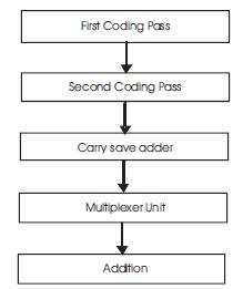
Figure 2. Flow diagram representation of Coefficient Generator
The reconfigurable pulse shaping FIR filter for digital up converter has been designed and simulated using Xilinx. The considered parameters are area and speed. The serial input data is given to data generator to sample the input data based on selection lines of multiplexer and produced the sampled output. In coefficient generator, first coding pass, second coding pass, partial product generator, multiplexer unit and addition operations are performed. The output from the data generator is given as the input to the coefficient generator. Each block in the coefficient generator produces the 16-bit output. The output from the coefficient generator is given as the input to the coefficient selector block to steer proper data based on selection lines. Finally, the final accumulation block produces the filter output by adding all the outputs. The output for each block is described and shown below.
Figure 3(a) shows the simulation result of first coding pass of coefficient generator. In this, four 16-bit filter coefficients given as the inputs to the multiplexer 0000000000111111, 0000000000101101, 00000001000011, 0000000001011110, 0000000001010011, 0000000000100001 and the given selection line is 1 that produces the output as 0000000000101101, 0000000001011110, 0000000000100001.
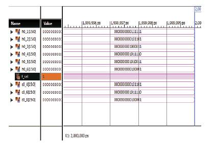
Figure 3(a). First Coding Pass of Coefficient Generator
Figure 3(b) shows the simulation result of Second coding pass of coefficient generator. In this, the output filter coefficients from the first coding pass is given as the inputs to the second coding pass. The inputs are then multiplexed and produce the output which depends on the selection line. For example , the given inputs are 00000000000010111, 0000000000111000, 0000000000111110 and the given selection line is 01 that produces the output as 0000000000111000.
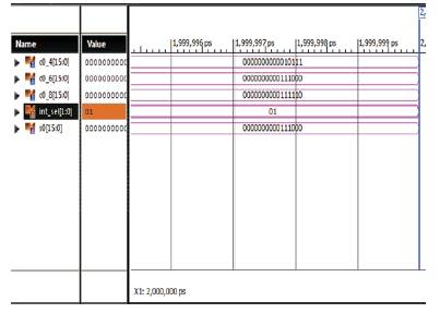
Figure 3(b). Second Coding Pass of Coefficient Generator
Figure 3(c) shows the simulation result of carry save adder of coefficient generator. In this, the output from the Second Coding Pass block is then multiplexed depending on the selection line to form coded coefficient. Then carry save adder is used for the multiplying the input and filter coefficient to produce partial product output.
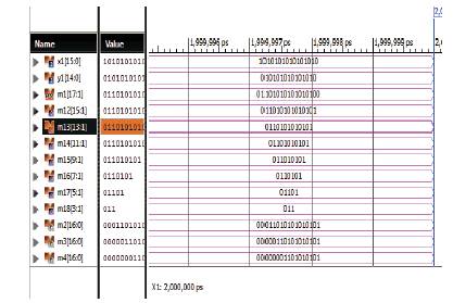
Figure 3(c). Carry Save Adder of Coefficient Generator
Figure 3(d) shows the simulation result of coefficient selector. In this, the output from the multiplexing and addition unit is given as the input of the coefficient selector which performs the AND operation between the output of multiplexer, addition unit and coefficients from the coefficient generator block. Then AND operation output gets multiplexed and produces the output depending on the selection lines.
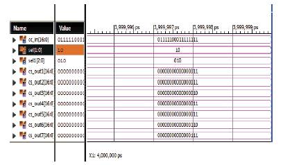
Figure 3(d). Coefficient Selector
Figure 3(e) shows the simulation result of multiplexer and final addition unit. In this, that, depending on the coded coefficient, the multiplexers will select the input data from the Partial Product Generator block and then addition unit performs the task of summing all the outputs of Partial Product Generator and produces the output. The output gets varied depending on the sign magnitude. Figure 3(f) shows the simulation result of overall designed pulse shaping FIR filter architecture output.
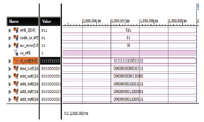
Figure 3(e). Multiplexer and Final Addition Unit
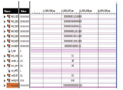
Figure 3(f). Final Filter Output
Figure 3(g) shows the RTL schematic output of the designed pulse shaping FIR filter architecture output.
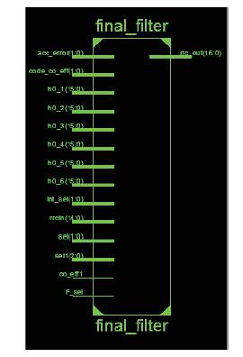
Figure 3(g). RTL Schematic Diagram of Filter
Table 1 shows the resource utilized by the RRC filter. It indicates the overall area consumption of the designed filter.
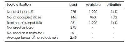
Table 1. Resource utilized by the designed PS-FIR filter
In this paper, pulse shaping FIR filter such as root-raised cosine filter was designed for multistandard digital up converter. The two bit binary common sub-expression based binary common sub-expression elimination algorithm is used to ignore the occurrences identical bit pattern. So, the number of additions and multiplications were reduced while using this technique. Carry save adder has been used to generate the partial product that reduced the area and parallel increased the speed. From the result it is concluded that, the power consumption of the designed filter is 0.052 which has been obtained using Xilinx ISE 12.1. In future, this designed filter will be implemented on FPGA Spartan-3E with the reduction of multiplexer's count. Further, this will improve the area and power consumption.