Figure 1. Basic Structure of the proposed Comparator
A new CMOS dynamic comparator using dual input, single output differential amplifier as latch stage suitable for high speed analog-to-digital converters with High Speed, low power dissipation and immune to noise than the previous reported work is proposed. Back to-back inverter in the latch stage is replaced with a dual-input single output differential amplifier. This topology completely removes the noise that is present in the input. The structure shows lower power dissipation and higher speed than the conventional comparators. The circuit is simulated with 1V DC supply voltage and 250 MHz clock frequency. The proposed topology is based on two crosses, coupled differential pairs positive feedback and switchable current sources, has a lower power dissipation, higher speed, less area, and it is shown to be very robust against transistor mismatch, and noise immunity. The simulation results will be shown on the W-Edit; average power consumption is in the T-spice.
Comparators are most probably second most widely used electronic components after operational amplifiers in this world. Comparators are known as the 1-bit analog-to digital converter and for that reason they are mostly used in large abundance in A/D converter. In the analog-todigital conversion process, it is necessary to first sample the input. This sampled signal is then applied to a combination of comparators to determine the digital equivalent of the analog signal. The conversion speed of the comparator is limited by the decision making response time of the comparator. As the comparator is one which limits the speed of the converter, its optimization is of utmost importance. In today's world, where demand for portable battery operated devices is increasing, a major thrust is given towards low power methodologies for high speed applications. This reduction in power can be achieved by moving towards smaller feature size processes. However, as we move towards smaller feature size processes, the process variations and other non-ideals will greatly affect the overall performance of the device. One such application where low power dissipation, low noise, high speed, less hysteresis, less offset voltage are required is Analog to Digital converters for mobile and portable devices. The performance limiting blocks in such ADCs is typically interstage gain amplifiers and comparators [1], [3], [6]. The accuracy of such comparators, which is defined by its offset, along with power consumption, and speed is of keen interest in achieving overall higher performance of ADCs. In the past, pre-amplifier based comparators have been used for ADC architectures such as flash and pipeline [8]. The main drawback of pre-amplifier based comparators is the more offset voltage. To overcome this problem, dynamic comparators are often used that make a comparison once every clock period and require much less offset voltage. However, these dynamic comparators suffer from large power dissipation compared to pre-amplifier based comparators. The main problem with all these dynamic comparators is the output signal of the latch stage is fluctuating during clock transition [11]. This is happening due to the presence of noise in input terminals. In this paper, the authors have designed all type of comparators.
In this Dynamic comparator design, there will be two phases, one is Reset phase when Clk=0 and then Latch Phase when Clk=1.
The rest of the paper is organized as follows. The necessity of the work is discussed in Section 2 and in Section 3, the design process of the work is presented in detail. In Section 4 the final structure of the design is presented. The performance results of the work and analysis are presented in Section 5 and the conclusion is followed by it.
Traditional operation require at least one DC bias current. As technology size has decreased, low power, high gain amplifier design has become more challenging for designers. Since transistor threshold voltage generally doesn't decrease as fast as feature size and the power supply voltage, many cascaded or folded designs are not possible with reduced voltage supply. Given that the reduction in headroom reduces the ability to cascade devices, low voltage high-gain amplifiers are commonly built by expanding outward, using two or even three cascaded amplification stages. These multi-stage cascaded designs require the designer to take extra measures to ensure amplifier stability, and, depending on the topology, can be very challenging or complex to stabilize. Most stabilization schemes require additional compensation capacitors and/or nulling resistors, which use additional silicon area, and can decrease circuit bandwidth; However, these compensations reduce power supply voltage, and the increasing demand for low power consumption make sub-threshold operation and design a more viable alternative when a reduction in bandwidth is acceptable. Operation in the sub-threshold region causes the drain current to increase exponentially with VGS as opposed to quadratically in the saturation region. The disadvantage with sub-threshold operation is the reduction in amplifier driving current, and the loss of ability to quickly drive large capacitive loads.
In this paper, an inverter-based operational amplifier topology and operation and design principles are discussed and evaluated. They use two previously used figures of merit to objectively compare various aspects of the different circuit topologies. The authors conclude that the inverter-based differential amplifier topology with current starving provides one of the best circuit topologies for energy efficiency.
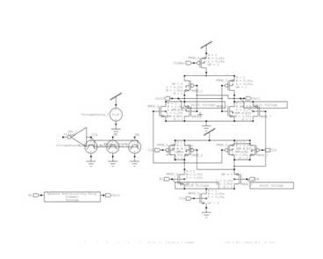
A high speed latched comparator using [5] positive feedback based, back to back latch stage, suitable for pipelined Analog to Digital converter, with reduced delay and high speed is proposed. During the RESET PHASE, when Clk is LOW ( Clk =0), transistor NMOS_5 is in off state and PMOS transistors PMOS_3, PMOS_6, PMOS_7, are in one state. Transistors NMOS_1 and NMOS_2 are in cutoff mode. Switching transistors PMOS_3, PMOS_9, PMOS_4, and PMOS_10 will charge the drains of transistors NMOS_ 1 and NMOS_2 and the output nodes Outp and Outn towards Vdd. During the REGENERATION PHASE, when Clk is HIGH ( Clk =1), the process starts by turning the transistor NMOS_3 on and immediately an current 'I' starts to flow and the drain of transistor NMOS_3 starts to discharge towards the ground (Gnd). In this succession the differential input transistors NMOS_3 and NMOS_4 are turned on. The currents of transistors NMOS_1 and NMOS_2, (at the drain terminal) will start to pull the output nodes Outp and Outn towards Gnd. Due to the difference of voltages between the input signals, the current at the drain terminals of transistors NMOS_ 3 and NMOS_4 will be different. Now in the regeneration mode the output node are discharging towards Gnd and pmos transistors PMOS_1 and PMOS_2 will come in saturation mode as the voltage at the output nodes falls below. The design is simulated using 0.25μm CMOS Technology using Tanner EDA Tools. The proposed design exhibits reduced delay and high speed with a 5.0 V supply. This design can be used where high speed and low propagation delay are the main parameter schemes, which have been improving with the usage of active compensation networks.
The proposed comparator (Figure 1) provides better input offset characteristic and faster operation in addition to the advantages of those comparators such as less kickback noise, reduced clock load and removal of the timing requirement between Clk and Clkb over a wide common mode and supply voltage range. The overall area is small even though the number of transistors is more. It is because the widths of transistors are optimized without compromising the speed and performance of the comparator. For its operation, during the pre-charge (or reset) phase (Clk=0V), both PMOS transistor PMOS_6 and PMOS_7 are turned on and they charge Di node capacitance to VDD, which turn both NMOS transistor NMOS_1 and NMOS_2 of the inverter pair on and Di' nodes discharge to ground. Sequentially, PMOS transistor PMOS_1, PMOS_2, PMOS_6 and PMOS_7 are turned on and they make Out nodes and SW nodes to be charged to VDD while both NMOS transistors NMOS_4 and NMOS_3 are being off. During the evaluation (decision-making) phase (Clk=VDD), each Di node capacitance is discharged from VDD to the ground in a different time rate proportional to the magnitude of each input voltage. As a result, an input dependent differential voltage is formed between Di+ and Di- node. Once either Di+ or Di- node voltage drops down below around VDD−|Vtp|, the additional inverter pairs PMOS_1/ NMOS_1and PMOS_2/ NMOS_2, invert each Di node signal into the regenerated Di' node signal. Then the regenerated and different phased Di' node voltages are amplified again and relayed to the output-latch. The additional Feedback transistors NMOS_% and NMOS_6 are used for reducing the static loss effect, which was suffered by the earlier comparator design. The terminology for various degrees of inversion is described.
Figure 1. Basic Structure of the proposed Comparator
In digital circuits, sub threshold conduction is generally viewed as a parasitic leakage in a state that would ideally have no current [9] In micro power analog circuits, on the other hand, weak inversion is an efficient operating region, and sub threshold is a useful transistor mode around which circuit functions are designed. Figure 2 shows the main idea Dual Tail Inverter based Comparator Design with Sub Threshold Voltage.
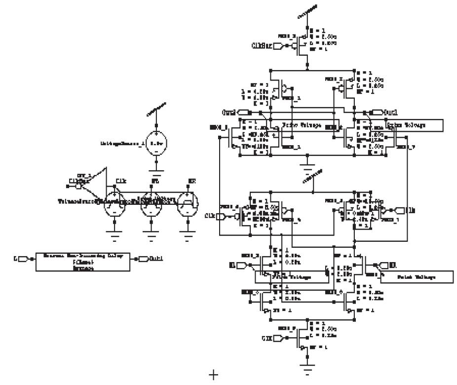
Figure 2. Main Idea Dual Tail Inverter based Comparator Design with Sub Threshold Voltage
In the past, the sub threshold conduction of transistors has usually been very small in the off state, as a gate voltage could be significantly below the threshold, but as voltages have been scaled down to transistor size, sub threshold conduction has become a bigger factor. Indeed, leakage from all sources has increased. For a technology generation with threshold voltage of 0.2 V, leakage can exceed 50% of total power consumption.
The reason for a growing importance of sub threshold conduction is that the supply voltage has continually scaled down, both to reduce the dynamic power consumption of integrated circuits (the power that is consumed when the transistor is switching from an on-state to an off-state, which depends on the square of the supply voltage), and to keep electric fields inside small devices low, to maintain device reliability. The amount of sub threshold conduction is set by the threshold voltage, which sits between the ground and the supply voltage, and so has to be reduced along with the supply voltage. That reduction means less gate voltage swings below threshold to turn the device off, and as sub threshold conduction varies exponentially with gate voltage (see MOSFET: Cut-off Mode), it becomes more and more significant as MOSFETs shrink in size.
Sub threshold conduction is only one component of leakage: other leakage components that can be roughly equal in size, depending on the device design, are gateoxide leakage and junction leakage. Understanding sources of leakage and solutions to tackle the impact of leakage will be a requirement for most circuit and system designers.
To reduce the sub threshold effect here they propose the stacking scheme an a design of the inverter based amplifier.
The inverter-based amplifier topology shown in Figure 3 uses CMOS inverters as the amplifier input. This input stage design has the advantage of combining the transconductance of the n and p transistors.
Figure 3. Inverter Based Amplifier Design
This combination of the two trans-conductances should provide 6dB increase in gain over a traditional common source, amplification stage, with approximately the same DC bias current. When this architecture is implemented with a standard supply voltage (>2vt), the overall trans conductance can be increased significantly depending on how transistors in the inverters are sized, and the resulting current through the inverter. High current through the inverter allows significantly higher bandwidths to be achieved. Another advantage of this topology is an increase in output swing and linearity when compared to a traditional common source or cascode amplifier if the respective trans- conductances of the p and n type transistors are approximately equal in magnitude. For noise, the inverter-based topology offers lower equivalent noise resistance compared to the equivalent common source topology. PMOS_5, PMOS_6 and NOMS_5 and NMOS_3 constitutes the stacking scheme for the comparator which reduces the sub-threshold (Figure 4) effect of a comparator by providing high resistance in the off region. PMOS_3 / NMOS_1 and PMOS_4/NMOS_2 are the inverter pairs through which differential inputs are fed across the outputs, the latch network was connected to PMOS_1/NMOS_4 and PMOS_2 / NMOS_6, which act like a latch network, which will increase the gain factor and decrease the delay of the comparator (Figure 5). The cross coupled pair provides positive feedback and therefore a negative resistance of -2/gm3.
Figure 4. Inverter based amplifier design with reduced Sub threshold
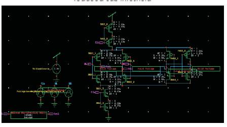
Figure 5. Inverter Based Amplifier with Latch network across
The results are compared with the existing technique. Table 1 shows the performance of the comparison of existing and proposed methods. The active device has considerably increased, when compared to the proposed methods. The area of the proposed works have got comparatively increased with the existing methods.
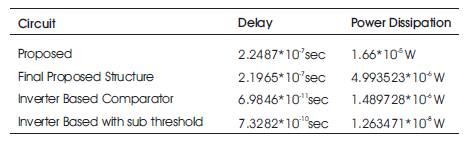
Table 1. Performance Results
In this paper, we presented a comprehensive delay analysis for clocked dynamic comparators and expressions were derived. Two common structures of the conventional dynamic comparator and conventional double-tail dynamic comparators were analyzed. Dynamic latched comparator was designed that works with high speed and low power consumption when compared to double tail latched comparator and pre amplifier based clocked comparator [13]. For comparison, the authors provided analog input to the comparator and the output was digital. The simulation results show that the proposed circuit can operate at higher speed with low power dissipation than the other two comparators. Also, based on theoretical analyses, a new dynamic comparator with low-voltage low-power [2] , [4], [7], [12] capability was proposed in order to improve the performance of the comparator. Post-layout simulation results in TSNC025. CMOS technology confirmed that the delay and energy per conversion of the proposed comparator is reduced to a great extent in comparison with the conventional dynamic comparator and double-tail comparator.