Introduction
The semiconductor technology is growing in a faster rate in the world. The major thing in this is there are many issues due to uncertainties, which may be the speed, area and may be the IO issues. To speed up the mechanism, generally we prefer parallel technique. Here the main purpose of this paper is to increase the performance and reduce the cost of the setup. This paper aims to enhance the design for the IO analysis of the memory interface of the CPU and develop the high speed IO characterization methods. Actually here we design the new setup that will reduce the cost around some dollars. And as per the time it will reduce by a factor of 1/8th means and the speed will be increase by a factor of 8 of the previous speed.
1. Literature Survey
This paper is about how advantageous it is when compared to the older version, and as there is increase in the speed of the IO operation and it saves money and time. Previously they are supposed to use the serial data acquisition devices, but now we are implementing parallel data acquisition methodology to reach our requirements. This survey indicates how this paper is appropriate to increase the performance with respect to the cost and speed from the below graphs (Figure 1 to Figure 4). The variation in the time spent and the cost is given in the different plots.
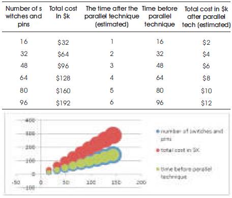
Figure1. The plot of the cost and time with respect to switches and pins for older design

Figure 2. Comparison in terms of time

Figure 3. The plot of the cost and time with respect to switches and pins for new design (estimated)
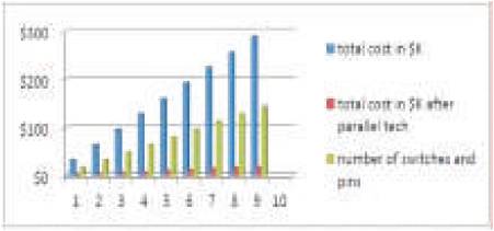
Figure 4. Comparison in terms of cost
2. New Methodology
Figure 5 shows the block diagram of the new design. Here we are using the NI USB 6008 for the interface between the PC and the PCB of the constant current source design.
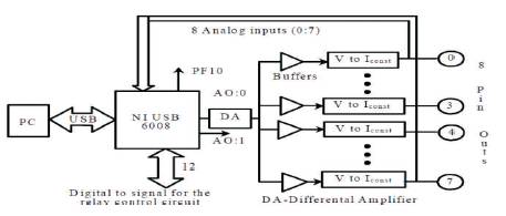
Figure 5. Block Diagram of New Design
Here we need to find out the ON Resistance of the pull up and pull down resister of the pin out which we use to measure the voltage across it by sending the constant current through it. After sending the constant current through the pin out, we can measure the output voltage from that point. Then we can store that value in the memory from the FIFO of the NI USB 6008. Here the main task is to design the constant bipolar current source which is based on the pin out condition. Internally it has pull up and pull-down transistors. These transistors are ON once at a time, based on the input that it exited. If the input is high, then the pull down is going to be in ON condition and it fed the R of the ON transistor. And the current that is fed into that resister acts as a current source. If the input is low then the pull up is going to be in ON condition and it fed the up R of the ON transistor. And the current that is fed from that resister acts as a current sink. The main parts of the design are as follows:
- National Instruments USB-6008
- Differential Amplifier(DA)
- Constant current source
- Voltage follower
- Relays
2.1 National Instruments USB-6008
The NI USB-6008 provides connection to eight single-ended analog input (AI) channels, two analog output (AO) channels, 12 digital input/output (DIO) channels, and a 32- bit counter with a full-speed USB interface.
2.2 Firmware
The firmware on the NI USB-6008 refreshes whenever the device is connected to a computer with NI-DAQmx. NI-DAQmx automatically uploads the compatible firmware version to the device. The firmware version may be upgraded when new versions of NI-DAQmx release, the pin out of the NI USB-6008. Analog input signal names are listed as single-ended analog input name, AI x, and then differential analog input name, (AI x+/–) (Figure 6).
2.3 Bipolar Constant Current Source
Current source: An ideal current source, I, is one driving a resistor, R, and creating a voltage V. A current source is an electronic circuit that delivers or absorbs an electric current which is independent of the voltage across it. A current source is the dual of a voltage source. The term constant-current sink is sometimes used for sources fed from a negative voltage supply. Figure 7. Bipolar Constant Current Soure/Sink.
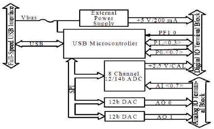
Figure 6. Block Diagram of NI USB-6008
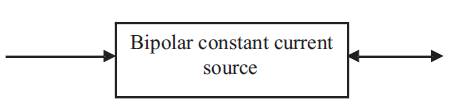
Figure 7. Bipolar Constant Current Soure/Sink
Current sources and sinks are analysis formalisms which distinguish points, areas, or volumes through which current enters or exits a system. While current sources or sinks are abstract elements used for analysis, generally they have physical counterparts in real-world applications; e.g. the anode or cathode in a battery. In all cases, each of the opposing terms (source or sink) may refer to the same object, depending on the perspective of the observer and the sign conversion being used; there is no intrinsic difference between a source and a sink.
- A source is a flow of current into the load.
- A sink is a flow of current from the load.
The constant current is given by
"Iout = [(R2 + R3)/(R1*R3)]*Vdiff “
3. Tools Used
The tools are Python and Multisim. Here python is used to develop the script and Multisim is used to simulate the analog circuits.
3.1 The Python Programming Language:
The programming language used is Python. Python is an example of a high-level language; other high-level languages you might have heard of are C, C++, Perl, and Java. There are also low-level languages, sometimes referred to as “machine languages” or “assembly Languages”. Loosely speaking, computers can only run programs written in low-level languages. Low-level languages are used only for a few specialized applications. Two kinds of programs process high-level languages into low-level languages: interpreters and compilers. An interpreter reads a high-level program and executes it, meaning that it does what the program says. It processes the program a little at a time, alternately reading lines and performing computations. A compiler reads the program and translates it completely before the program starts running. In this context, the high-level program is called the source code, and the translated program is called the object code or the executable. Once a program is compiled, you can execute it repeatedly without further translation. Alternatively, you can store code in a file and use the interpreter to execute the contents of the file, which is called a script. By convention, Python scripts have names that end with .py.
3.2 NI Multisim
NI Multisim (formerly MultiSIM) is an electronic schematic capture and simulation program which is part of a suite of circuit design programs, along with NI Ulti board. Multisim is one of the few circuit design programs to employ the original Berkely SPICE based software simulation. Multisim was originally created by a company named Electronics Workbench, which is now a division of National Instruments. Multisim was originally called Electronics Workbench and created by a company called Interactive Image Technologies. At the time it was mainly used as an educational tool to teach electronics technician and electronics engineering programs in colleges and universities. National Instruments has maintained this educational legacy, with a specific version of Multisim with features developed for teaching electronics.
Conclusion
- Complexity is reduced by replacing the Keithley switches by the new design.
- Speed of the operation is increased by a factor of 8.
- Cost is effective when compared to the older design.
Future Scope
In the second phase the author is going to design and implement circuit diagram of his new design and the programming part. That will be used to characterize the IO characteristics of the memory interface of CPU practically.
Acknowledgment
The author express his truthful obligations towards his guide, Mr. V. Murali Praveen, M.Tech, Assistant Professor in ECE Dept and to his Project Coordinator Mr. G. Rajesh, M.E,(P.hd) Associate Professor, ECE Dept., for their clever guidance and useful suggestions, which assisted him in the project work.