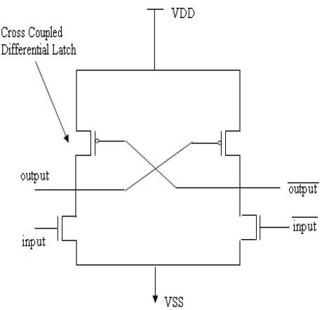
Figure 1. Adiabatic logic Inverter
Adiabatic Logic styles in low power VLSI design have been examined for many years to achieve predictable low power design success. In this paper, the authors present a comprehensive literature review pertaining to the state-of-the-art issues in adiabatic logic designs and also focus on primary developments in this field that have taken place in the low power design. Various research papers and application notes have been referred to, for clear understanding of adiabatic logic designs on low power solutions. Major focus of this paper is to identify the gaps of the adiabatic logic designs and to narrow down the problems and requirements for its practical usage in semiconductor industries. Enough designs and methods have been proposed over last few decades, but the implementation of this logic, triggers the designer in various open points, which restricts further stems. This paper highlights the major open points and gives the solution for further design requirement to implement the adiabatic logic in semiconductor industries.
Over the past few decades, low power design solution has steadily geared up the list of researcher's design concerns, over the rising cost of energy, and an increasing sensitivity to green practices, low power consumption and the like, have become a major concern for design engineers. Various classical approaches are available to designers looking to reduce power consumption, by means of utilizing sleep/standby modes, shrinking of wafer size, reduction of node capacitances and switching frequencies. These techniques are not fit enough to meet today's power requirement. Even though, the required power dissipation and cost has been achieved by lithography, these approaches deliver only incremental improvements. The ceaseless need for low-power circuits is now motivating designers to explore new options in circuit designs. Two decades-old circuit styles, adiabatic and asynchronous style of approaches now assure to offer a possible solution to low power circuit design, discussed by Ajluni (2009) in [1].
In commercial utilization of these techniques, continuous improvement and development has to be done. Most research has focused on building adiabatic logic, which is a promising design for low power applications. In the following sections, the various techniques of adiabatic logic styles are highlighted for low power applications. Will these approaches provide the answer to the ongoing low power issues, is a mighty interrogation. So let us take a closer view.
“Adiabatic” is a term of Greek origin which spent most of its history related with classical thermodynamics. It refers to a system in which a transition occurs without energy (usually in the form of heat) being either lost to or gained from the system. In the context of electronic systems, rather than heat, electronic charge is preserved. Adiabatic logic is viewed on issues related with the thermodynamics of computation. By considering this branch of physics that usually looks at mechanical engines and applying it to computing engines, research areas such as reversible computation as well as adiabatic logic have been developed. By moving to a computing paradigm that is reversible, energy can be reprocessed from a computing engine, and reused to perform further calculations. The benefit of adiabatic logic is that energy can be recycled by means of storing for reuse, which reduces the amount of energy drawn directly from the power supply, discussed by Koller and Athas (1992), in [2]. Thus, an ideal adiabatic circuit would operate without the loss or gain of electronic charge. It is a novel low-power design style to achieve low energy dissipation by restricting current, so that it flows across a device with very low voltage drop for recycling the energy stored on the device's capacitors. This style of logical approach differs from CMOS circuits, which dissipate energy during switching. There are two basic types of adiabatic circuits, fully adiabatic and quasi adiabatic. In fully adiabatic circuits, charge from a discharging capacitor is used to charge the capacitance from the next stage. The quasi adiabatic circuits reclaim part of the energy spent during circuit operation and reprocess the retrieved energy for subsequent operations.
In [3], the circuit of an adiabatic logic inverter is discussed by the author Gary K. Yeap (1998), which is represented in Figure 1. The circuit employs fully differential logic signals and requires a four phase dynamic operation to compute a single Boolean logic function as represented in Figure 2. There are noticeable differences in this circuit as compared with conventional static or dynamic CMOS circuit. The most apparent difference is that the supply voltage is no longer constant. A periodic ramp signal is used to power the circuit. The power signal also acts as the clock signal of the circuit because it synchronizes the circuit operations. Each logic bit requires signals for inputs and outputs. The P-transistor pair provides positive feedback to the output signals, like a cross-coupled inverter. The two Ntransistors of the inverter acts as evaluation transistors during logic computation, much like the dynamic CMOS logic. In general, the N-transistors form a serial-parallel network to perform a non-trivial Boolean computation. An adiabatic circuit with full complementary feedback is shown Figure 3.
Figure 1. Adiabatic logic Inverter
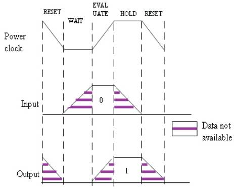
Figure 2. Four phases of adiabatic logic
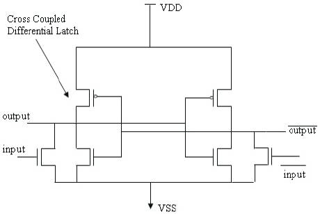
Figure 3. Adiabatic circuit with full complementary feedback
The four phases of operation are detailed below:
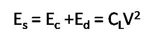
The equivalent circuit for the conventional dynamic or static CMOS logic is shown in Figure 4 (a). The energy Es dissipated during a charging and discharging cycle is,
regardless of the resistor Rs . Ec , Ed is the energy dissipated due to charging and discharging of the capacitor CL . The charging and discharging of the parasitic output capacitance in the adiabatic logic circuit occurs in the EVALUATE (RESET) phase. The equivalent circuit for the charging phase is shown in Figure 4 (b), where Ra is the resistance of the charging P-transistor.
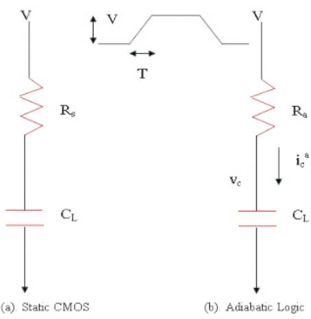
Figure 4. Equivalent circuit when charging output capacitance
Assuming that the time constant of the circuit Ra CL is much smaller than the voltage ramp periods T i.e.,
This means that the voltage at the capacitor closely follows the supply voltage and the potential difference across Ra is very close to zero.
The voltage at the capacitor Vc is also a constant ramp with slope V/T where V is the swing of the supply voltage and T is the power-clock phase period. The charging current of the adiabatic circuit is
The energy dissipated in the resistor is given by,
The equivalent circuit for the discharging is similar to that of charging except that the supply voltage ramps down. Therefore, equations (3) and (4) also apply to the discharging phase and the energy dissipation of a fourphase computation cycle of the adiabatic logic is
The difference between equations (1) and (5) is the factor (2 Ra CL )/ T. In both cases, the resistance of the charging and discharging circuit dissipates the electrical energy from the power supply only. Capacitors only act as energy storage devices and do not dissipate power. In CMOS circuits where the supply voltage is constant, a large voltage is exerted across the resistor, when charging cycle begins, resulting large current and energy dissipation. However, in the adiabatic logic, a slow ramping power signal is used to charge the capacitor. The voltage across the resistor Ra is much smaller compared to that of the static CMOS circuits, resulting in less energy dissipation. Consider the energy 2 stored in the capacitor 0.5 CL V2 and the energy dissipated during charging or discharging Eca . Because Ra CL << T, we have,
The energy stored in the capacitor is more than that dissipated by the resistor during charging or discharging. This suggests that during discharging, some energy stored in the capacitor is actually returned to the energy source. In the adiabatic logic circuit, the power supply is implemented by a resonant circuit that can reclaim the electrical energy stored in the capacitor and reuses it in the next cycle. The efficiency of the adiabatic and static CMOS logic is illustrated in Figure 5. The energy efficiency of the static CMOS is independent of the operating frequency. However at low operating frequencies, adiabatic circuits are more energy efficient than static CMOS circuits (Yeap, 1998).
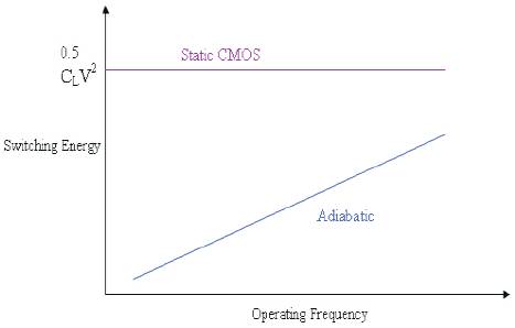
Figure 5. Switching energy of static CMOS and adiabatic logic
In adiabatic logic, the main design changes are to be focused in power clock which plays the vital role in the principle of operation. Each phase of the power clock gives user to achieve the two major design rules for the adiabatic circuit design.
1. The inputs must be valid during the charging/ discharging process.
2. Make sure every node is reset to the original stage before performing the next operation.
1. The inputs must be held static throughout the charging and discharging of capacitances.
2. Ensure high resistance results in more energy consumption.To overcome the power and area requirements of the computational complexities, the dimensions of transistors are shrunk into the deep sub-micron region and predominantly handled by process engineering. Driven by tremendous advances in lithography, the 65nm process technology node featuring approximately 28nm transistors is in vogue right now in high volume production. Moreover, the technology migration has become much costly for process the design in terms of its physical design. Developers are forced to bare the tool cost in order to achieve the low power requirements. The transistor cost versus lithographic tool cost, is given in the silicon technology future road map. It is noted that transistor cost has decreased seven orders of magnitude, whereas tool cost has increased. Thus, the alternate solution of process engineering is a great welcome, as discussed (Kishore, Somasundareswari, Duraisamy and Pradeep, 2010).
The equivalent names that have been used by various authors to refer to adiabatic logic systems include “Charge recovery logic”, “Charge recycling logic”, “Clock-powered logic”, “Energy recovery logic” and “Energy recycling logic” [8-20]. The biggest problem of implementing the adiabatic logic is the logical approach of the design methodology, which has to be totally renewed by new approach. It is the critical point that semiconductor industries look forward the amount of resource requirement in new strategy. At initial focus, it may not be possible for the complete change in the logical approach, and it is almost to reset the past five decades of progress in the semiconductor industries. To be in deep drill to analyze the fitment of adiabatic, the following question may arise, “What are the minimum changes adopted by semiconductor manufacturer for the fitment of adiabatic?”
Since the early 70's, the Moore's law has been intensively performed a significant role in semiconductor industry. With the help of transistor scaling, one obtains a superior performance to cost ratio of products, which leads an exponential growth of the semiconductor market, which allows further investments in semiconductor technologies which will render further scaling. Over the decades, the wavelength and feature size have been changed dramatically, as represented in Figure 6.
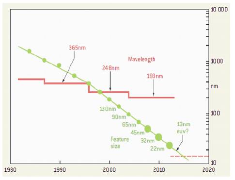
Figure 6. Improvement on Wavelength and Feature size
Due to the internal, external capacitance and resistance of the semiconductor, external parasitic will be much more influenced while reducing the wafer size. It causes overlapping of both parasitic and channel parameters. It is called parasitic dominance and thus, the industries should look for the alternate material or solution to maintain the internal resistance which decreases with respect to the reduction of wafer size. The channel, parasitic resistance Vs feature size and channel, parasitic capacitance Vs feature size are shown in Figures 7 & 8. The physical design is a major challenge in reducing the feature size. But power consumption is a critical issue in the system performance and is listed as one of the main three challenges in International Technology Roadmap for Semiconductor. As quoted in [5], low power design can be exploited at various levels, e.g., system level, architecture level, circuit level, and device level (Wang, 2009).
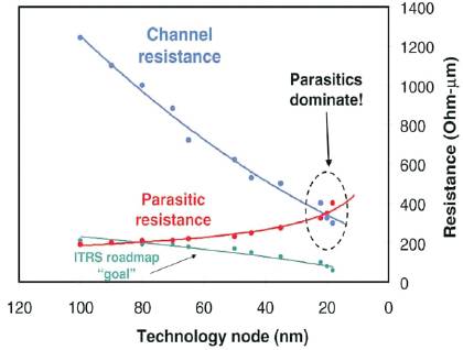
Figure 7. Channel Resistance Vs Feature size
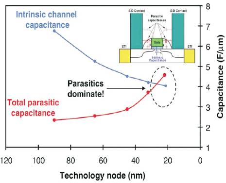
Figure 8. Channel capacitance Vs feature size
Fury (2012) discussed the transistor cost (cost per million gates $) for various process technology nodes in [6] and it is illustrated in Figure 9. Here, transistor cost is not scaling with node for 28nm, 20nm and 14nm; they are all falling to the same normalized cost per transistor, as did 55nm and 40nm. Moore's law describes the requirement of the transistors for VLSI design; it gives the empirical observation that component density and performance of integrated circuits, doubles every year, which was then revised to doubling once in every two years. With the help of the scaling rules, smart optimization can be achieved by means of timely introduction of new processing techniquesin device structures, and materials.
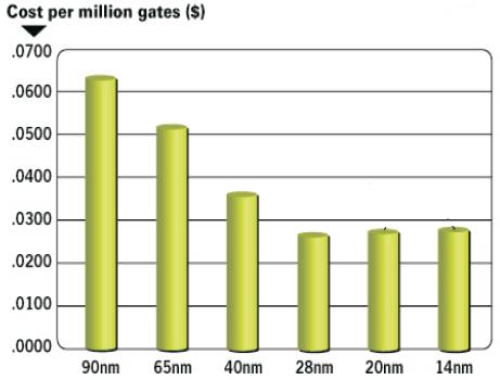
Figure 9. Transistor cost for various process technology nodes
In earlier investigation of semiconductor process technology, low power CMOS design has been achieved mostly by shrinking of the wafer size. The performance against the EMC / EMI requirement of military grade is a great challenge in design requirements. The alternative technology or material is needed to overcome the saturation of the wafer shrinking in the semiconductor industries. Also these industries face problem in further reduction of the wafer size, in terms of parasitic dominance. Hence, the solution to avoid parasitic dominance is the ultimate focus which leads to search for an alternative solution. Various logics have been proposed by designers to reduce the power dissipation and permanent solution of this problem is of great interest. Meanwhile, the focus of adiabatic logic design was increased to fit this logic, but it has biggest implementation challenges in the semiconductor industry. Hence, this approach again decays the appreciation of the semiconductor manufacturer, reduces the adiabatic designer to do further improvement on this adiabatic fitment in the current technological corner.
The continuous logical implementations have grown, analyzed and proved that the adiabatic logic meets the best performance in terms of power dissipation, but, the compatibility of this logical design in the existing CMOS design is not well focused.
In [7], the reduction of dissipation in logic circuits with recovered energy logic (REL) had been investigated by the authors Hinman and Schlecht (1993) and a power supply/clocking circuit used to drive a REL circuit at up to 100 MHz had been described. In [8], charge recovery logic (CRL) and split-level charge recovery logic (SCRL) had been discussed by the authors Younis, Saed and Knight (1994), which resembles static CMOS gates followed by a transmission-gate with their power rails replaced by powerclock signals. In [9], the authors Kramer et al. (1994) discussed a diode-based complementary logic of adiabatic computing (2N-2N2D) with pairs of NMOS devices (designated by “2N”) and pair of diodes (designated by “2D”) to promote, a constant and data independent capacitive load to the clock, results the considerable amount of energy savings. In [10], adiabatic dynamic logic (ADL) had been designed by the authors Dickinson and Denker (1994) and achieved considerable amount of reduction in power consumption over conventional CMOS circuit design.
In [11], adiabatic pseudo-domino logic (APDL) structure by combining adiabatic theory and CMOS domino logic had been proposed by the authors Wang and Lau (1995) and recovered over 80% of the energy dissipated in conventional static CMOS logic design. In [12], a low-power clocked CMOS adiabatic logic (CAL) with integrated single ac power supply had been designed by the authors Maksimovic et al. (1997), by performing true and complementary logic functions, to present a constant capacitive load to the power clock generator. The authors Moon and Jeong (1996) proposed efficient charge recovery logic (ECRL) as a technique for low-energy adiabatic logic circuit and achieved four to six time power reductions with practical loading and operation frequency range [13].
In [14], 2nd order adiabatic computation with 2N-2P and 2N-2N2P logic circuits had been proposed by the authors Kramer et al. (1995) to achieve adiabatic power savings without costing much more either in terms of complexity or size. The authors Mateo and Rubio (1996) proposed a quasi-adiabatic ternary logic to diminish the expensive silicon area requirements. With this logic, the performance of a half adder was obtained with 65% of area saving with respect to adiabatic binary logic [15]. In [16], CMOS positive feedback amplifier, based on dual rail logic had been presented by the authors Vetuli, Pascoli and Reyneri (1996) to ensure high noise immunity and energy recovery process. The authors De and Meindl (1996 a, b) proposed the complementary adiabatic MOS (CAMOS) and fully adiabatic MOS (ADMOS) logic families, to provide the circuit implementations of quasi-adiabatic and quasiadiabatic- reversible computing. The authors also described the static and dynamic energy recovery logic families and achieved significant energy savings, compared with conventional static and dynamic CMOS [17, 18]. In [19], a pass-transistor adiabatic logic (PAL) with single power-clock supply had been designed by the authors Oklobdzija, Maksimovic and Lin (1997) and achieved considerable amount of energy savings. In [20], quasi-static energy recovery logic family (QSERL) using two complementary sinusoidal supply clock had been proposed by the authors Ye, Roy and Stamoulis (1997). QSERL multiplier was designed by the authors and achieved 37% of energy over static CMOS multiplier at 100 MHz. In [21], an improved input-isolation structure for APDL (adiabatic pseudo-domino logic) had been dealt by the authors Lau and Liu (1997) to provide a higher frequency performance with simple clock supplies and achieved a reduction of up to 75% in power dissipation. In [22], the authors Kwon and Chae (1998) proposed simple reversible energy recovery logic called feedback RERL and achieved considerable amount of energy savings.
In [23], adiabatic differential cascode voltage switch with complementary pass-transistor logic tree (ADCPL) had been proposed by the authors Lo and Chan (1998) and achieved power reduction of 50% to 70% by recovering the energy in the recovery phase of the supply clock in pipelined ADCPL carry look ahead adder. In [24], a 2:1 multiplexer with pass-transistor adiabatic logic with NMOS pull-down configuration had been designed by the authors Liu and Lau (1998) and achieved significant power savings. In [25], the authors Liu and Lau (1998) also proposed an improved structure for efficient charge recovery logic (IECRL) and achieved significant power performance than ECRL, coupled with an improved output waveform. In [26], a single-phase source-coupled adiabatic logic family (SCAL) had been described by the authors Kim and Papaefthymiou (1999) and designed an energy efficient SCAL adder.
In [27], the authors Takahashi and Mizunuma (2000) proposed an adiabatic dynamic CMOS logic (ADCL) circuit for super low power consumption and achieved considerable amount of energy savings. In [28], a complement type pass-transistor bootstrapped chargerecovery logic (CP-BCRL) had been presented by the authors Luo et al. (2001) and achieved efficient energy transfer/recovery, less energy consumption. In [29], two phase non-overlapping clock adiabatic differential cascode voltage switch logic had been proposed by the authors Suvakovic and Salama (2000), they addressed the issues related to resonant circuits and the design of sequential adiabatic logic circuits , preventing adiabatic system implementations from outperforming conventional CMOS designs in terms of energy efficiency. The authors Varga, Kovacs and Hosszu (2001a, b) proposed Efficient Adiabatic Charge Recovery Logic (EACRL) to eliminate non adiabatic loss during the charge phase. The authors also proposed an improved pass-gate adiabatic chargerecovery logic (IPGL) to offer efficient power consumption with moderate reversibility overhead for frequencies below 400 MHz [30,31]. In [32], a complementary pass-transistor energy recovery logic (CPERL) had been proposed by the authors Chang, Hung and Wang (2002) and designed a CPERL 10-stage inverter, which utilizes the bootstrapping technique and consumed 48.8% of energy dissipation at 125 MHZ.
In [33], a complementary pass-transistor adiabatic logic (CPAL) had been presented by the authors Jianping, Cen and Liu (2003). In this technique, complementary passtransistor logic was used for logic-evaluation and transmission gates for energy-recovery, to achieve significant energy transfer and low energy loss with complete elimination of non-adiabatic loss in the output loads. An inverter chain with this design had been performed and achieved 2.5 to 3 times more energy efficient than 2N-2N2P and 3 to 9 times less dissipative than the static CMOS for clock rates ranging from 25 to 300MHz. In [34], a modification of improved adiabatic pseudo domino logic (IAPDL) with reduction of one diode had been presented by the authors Widjaja and Lau (2003) and achieved considerable area savings and reduced power dissipation at lower supply voltages.
In [35], the authors Fischer et.al (2004) proposed the improved PFAL (I-PFAL) to enable significant reduction of the energy dissipation, in which, all n- and p-channel devices are swapped so that the delivered charge can be recovered through an n-channel MOSFET, which decreases the resistance of the charging path. In [36], the authors He, Tian, Tan and Min (2006) analyzed a quasi- static adiabatic logic family called 2N-2N2P2D to achieve higher power saving by eliminating redundant capacitive node charge/discharge. Compared to the 2N-2N2D logic, this design achieved 40 % power saving and up to 70 % as compared to the conventional CMOS logic. In [37], a quasi-static single-phase energy recovery logic (QSSERL) had been proposed by the authors Shun et al. (2007), by employing single sinusoidal supply-clock without additional voltages, which ensures lower energy dissipation and simplified clock design. The QSSERL adder was performed by the authors with only 56% of energy consumption as compared with its static CMOS counterpart at 10MHz. The authors Vijayakumar, Shanthanalakshmi and Gunavathi (2007a, b) proposed an efficient improved positive feedback adiabatic logic (IPFAL) to utilize the inherent nature of pipelining in the circuits with the help of fourphase power clock and recovered the stored charge from the load capacitance with reduced non-adiabatic losses in the circuit. The authors also proposed an efficient charge recovery positive feedback adiabatic logic (PFAL), by including an additional charge recovery path in parallel to the cross coupled PMOS transistors and attained energy efficient among adiabatic logic families [38, 39].
In [40], the authors Kumar, Tripathy and Tripathi (2009) discussed adiabatic flip-flops (D and JK) and a practical sequential circuit (4-bit shift register) was realized with adiabatic CPL. This adiabatic CPL D flip-flop achieved power savings of 81% with CPAL, 88% with 2N-2N2P logic and JK flip-flop achieved 13% to 68% with CPAL, 69% to 91% with 2N-2N2P logic for clock frequencies from 50 to 300 MHZ.
In [41], a family of adiabatic inverter, NAND gates, NOR gates, adder circuits and JK flip-flop had been proposed by the authors Reddy, Satyam and Kishore (2008) and achieved considerable energy savings as compared with CMOS circuits. In [42], an irreversible energy recovery logic (ERL) families called complementary energy path adiabatic logic (CEPAL) had been presented by the authors Gong et al. (2008) which inherits the advantages of quasi-static ERL (QSERL) family with improved driving ability and circuit robustness and achieved considerable energy savings. In [43], the authors Willingham and Kale (2011) proposed a ternary full-adder capable of reducing four input trits (ternary-digits) to two output trits with novel ternary adiabatic logic (TAL) family and achieved average power consumption of 216fW per addition, when operated at 1MHz.
In this section, the general focus on the progress of adiabatic logic design is discussed, which shows how the designs of adiabatic logic families have progressed over time. It is noted that most of these adiabatic logic designs have used synchronous clocking. To obtain all low power advantages from the adiabatic logic, power clock generator plays vital role in adiabatic circuits. The clock routing is also serious issue in the adiabatic circuits. Thus, to overcome the problems associated with clock generation and synchronous clock routing are of great interest.
Figures 10 and 11 shows the operational benefits of Synchronous clock system Vs Asynchronous clock system. The synchronous system utilize the clock source globally, i.e. single clock is shared and restored by the large number of logical gates in parallel, and here switching loss of the power clock generator is large as in the CMOS circuit operation. The simple structure of the pass-transistor logic makes it easy to adjust the sizing of transistors to get the desired charging and discharging time and hence the slope of the output control signal minimizes the power. In asynchronous clock system, the clock energy is locally stored in the control and regeneration (C&R) block and it has been used for subsequent gates, the loss of energy of each operation will be taken from its clock source. The control and regeneration part which controls and regenerate the energy, required for the next operation to the next logical block. The energy of the system will be circulating among the logical circuits and the minimum power is required from the power clock generator for the operation.
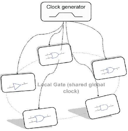
Figure 10. Synchronous supply Clock
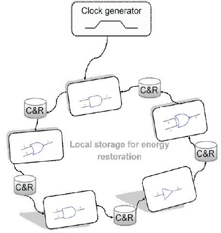
Figure 11. Asynchronous supply Clock
In general, the regenerated signal is stored and circulated between the C&R and logical part; thus, there is no powerreversal to the power clock system. It also helps to reduce the power clock system switching losses as discussed by Kishore et al. (2010).
It is a novel low-power design technique which combines the energy saving benefits of asynchronous logic and adiabatic logic, to introduce low power systems whose power dissipation is reduced in many ways. Like adiabatic circuits, asynchronous circuits are also a promising technology to focus low-power, highly modular digital circuits. One of the properties of asynchronous systems which make them useful in these applications are that circuits include a built-in insensitivity to variations in power supply voltage, with a lower voltage resulting in slower operation rather than the functional failures that would be seen if traditional synchronous systems were used. Another benefit is the fact that when an asynchronous system is idle, it will not utilize clock signals, whereas in synchronous systems, these clock signals are propagated throughout the entire system and convert energy to heat, often without performing any useful computations.
In contrast to synchronous circuits which operate according to clock timing signals, asynchronous circuits use handshaking between their components to perform all necessar y synchronization, communication and sequencing of operations. Asynchronous circuits fall into a number of different classes, each offering different advantages. The main privilege of this circuit is its low power consumption, stemming from its elimination of clock drivers and the fact that no transistor ever transitions unless it's performing a useful computation. A key deprivation of this circuitry is that the asynchronous control logic designed to implement the handshaking may represent an overhead in terms of silicon area and circuit speed.
The authors Willingham and Kale (2004, 2008 a,b,c) proposed "asynchrobatic" low-power logic design style to utilize the low-power benefits of an asynchronous controller to drive a wide data-path of quasi-adiabatic elements and achieved more efficient asynchronous data-path widths. The addition was performed in low-power asynchrobatic (asynchronous, quasi-adiabatic), sixteen-bit, radix-four, parallel-prefix adder circuit and achieved 69 pW, with 48.3 pW used by the control logic and 20.7 pW by the datapath. Also, a reversible, positive feedback adiabatic logic circuit had been presented by these authors by implementing the universal Toffoli gates, and achieved 63% reduction in energy losses. In, an asynchrobatic system that uses Euclid's algorithm to calculate the greatest common denominator of two numbers had been presented by the same authors and 16-bit implementation was performed with a power consumption of 3.257 nW [44-47].
In [48], asynchronous adiabatic logic had been proposed by the authors Arsalan and Shams (2007) to avoid the problems related to clock generation and synchronous clock routing in the adiabatic systems by utilizing the benefits of the adiabatic logic circuits with asynchronous logic systems.
Low power multiplier design using complementary passtransistor asynchronous adiabatic logic had been investigated by the authors Kishore et al. (2010), which exhibits low power and reliable logical operations comprising the benefit of both asynchronous systems with adiabatic benefits, compared with the conventional CMOS implementation, this design achieved energy savings from 50% to 74% for clock rates ranging from 100MHz to 300MHz.
In [49], the authors Kishore et al. (2011) proposed a low power full adder design using asynchronous adiabatic logic with complementary pass transistor. The addition was performed by this design and achieved energy savings from 15% to 80% for clock rates ranging from 1MHz to 200MHz.
In this study, the two research areas, adiabatic logic and asynchronous adiabatic logic are reported. They offered a different set of low-power benefits which they could convey to circuit design. From this study, it is observed that most of the adiabatic logic designs have used synchronous clocking. In order to achieve optimal low power benefits from the adiabatic logic, the robust design of power clock generator is of great interest. To get out of the problems related to power clock generator and clock routing, asynchronous supply of clocking is a great welcome. Asynchronous clocking is used to reduce the power clock system switching losses. Hence, asynchronous adiabatic logic is a novel idea to attempt to find a way to unify the low power benefits from these fields.
Demand for low-power designs will likely not end up anytime soon. Classical techniques can be used to address this demand, but with their incremental results, designers will need to investigate other options. Asynchronous adiabatic logic design styles now offer designers an alternate solution to dealing with the lowpower issues. As energy dissipation moves toward overwhelming all other design concerns, design styles like these will be critical to providing the energy efficiency that today's electronic systems require. Other than the design verification and power requirement of logic, designer have to analyze the interfacing possibility of the adiabatic circuits to the current CMOS world, this will improve the confidence on the asynchronous adiabatic usage in the real world.
In the following section, the authors suggest an approach for the usage of asynchronous adiabatic logic in more common way, with the low power requirement.
The interfacing possibility of the asynchronous adiabatic circuits to the current CMOS world is highlighted in Figure 12. The suggested asynchronous adiabatic logic output pad cells include mainly chip pads, electrostatic discharge (ESD) protection circuits, and multistage asynchronous adiabatic buffers that are used to drive the large load capacitances on the chip pads, along with asynchronous adiabatic power supply. Their structure is similar to conventional CMOS digital output pins except for the conventional CMOS inverters, which are replaced by the multistage asynchronous adiabatic buffers to reduce the energy dissipations on the large load capacitances.
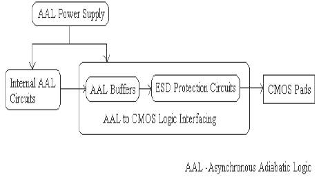
Figure 12. Schematic of AAL pad cells for driving CMOS chip pads
In order to reduce full-adiabatic energy dissipations on the output nodes and maintain high operation frequencies, enough large device sizes of the adiabatic buffers should be used for a large node capacitance on the chip pads, as stated by the authors Jianping et al. (2009) in [50]. This asynchronous adiabatic logic pad cells can be integrated in a chip with CMOS technology, which is a promising design solution for low power applications. Thus, this proposal will make more utilization of low power aspects in real world, by comprising the benefit of both asynchronous systems with adiabatic benefits.
Today's design engineers are focusing a growing need to conserve power. To meet low power requirements, they require a comprehensive, robust low power design services to help them meet their toughest design challenges. This paper is based on number of research articles published in the last two decades and periodic updates on adiabatic logic families, which will be useful as new practices continue to evolve in the field of low power design. The citations listed in this paper furnish a representative sample of current thinking pertaining to the future techniques of adiabatic logic on low power solutions. With the proposed AAL pad cells, asynchronous adiabatic logic of low power design will offer promising solution to implement this logic in semiconductor industries significantly.
Authors would like to thank all the researchers who have contributed in this field of research. The comments of anonymous reviewers, which have considerably helped to improve the quality of this paper, are also acknowledged.