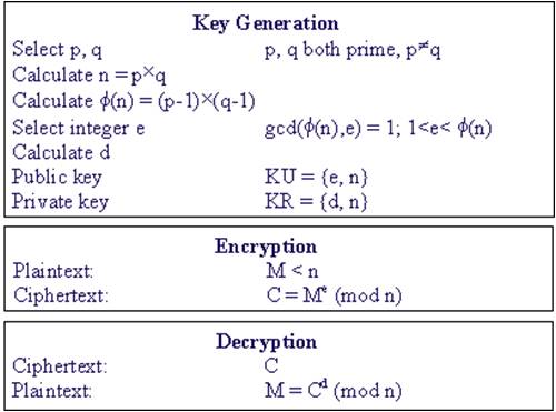
Figure 1. The RSA algorithm
The RSA system is widely employed in networking applications for good performance and high security. It supports the multiple key sizes like 128 bits, 256 bits, 512 bits. In this paper, The authors use Verilog code to implement a 16-bit RSA block cipher system. Therefore it can easily be fit into the different systems requiring different levels of security. The whole implementation includes three parts: key generation, encryption and decryption process. The key generation stage aims to generate a pair of public key and private key, and then the private key will be distributed to receiver according to certain key distribution schemes. The memory usage and overhead associated with the key generation is eliminated by the proposed system model. The cipher text can be decrypted at receiver side by RSA secret key. Verilog code is synthesized and simulated using Xilinx-ISE 12.1. It is verified that this architecture supports for multiple key of 128bits, 256bits, and 512 bits. Net list generated from RTL Compiler will be used to generate the IC layout. In this work, they have also developed an algorithm using LabVIEW 2010. LabVIEW (Laboratory Virtual Instrument Engineering Workbench) is a graphical programming language that uses icons instead of lines of text to create programs. Unlike text based programming language, LabVIEW uses the data flow programming, where the flow of data determines the execution. The flexibility, modular nature and ease to use programming is possible with LabVIEW, making it less complex.
Cryptography plays an important role in the security of data. It enables us to store the sensitive information or to transmit it across the insecure networks so that unauthorized persons cannot read it. The urgency for secure exchange of digital data resulted in large quantities of different encryption algorithms which can be classified into two groups: symmetric key algorithms (with private key algorithms) and asymmetric key algorithms (with public key algorithms) [1]. The asymmetric key algorithm requires two different keys, one for encryption and other for Decryption. The most common public key algorithm is RSA, named for its inventors Rivest, Shamir, and Adleman (RSA). The RSA algorithm is a secure, high quality, public key algorithm [2]. It can be used as a method of exchanging secret information such as keys and producing digital signatures.
However, the RSA algorithm is very computationally intensive, operating on very large (typically thousands of bits long) integers. It uses two numbers, e and d, as the public and private keys, and the two keys e and d have a special relationship to each other [7]. This paper describes the implementation of RSA encryption/decryption algorithm on FPGA using 128 bits key size.
The RSA algorithm was invented by Rivest, Shamir, and Adleman in 1977 and published in 1978. It is one of the simplest and most widely used public-key cryptosystems. Figure 1 summarizes the RSA algorithm.
The system architecture for key generation is shown in Figure 2. A random number generator generates 512-bit pseudo random numbers and stores them in the rand FIFO. Once the FIFO is full, the random number generator stops working until a random number is pulled out by the primality tester. The primality tester takes a random number as input and tests if it is a prime. Confirmed primes are put in the prime FIFO. Similarly to the random number generator, primality tester starts new test only when prime FIFO is not full. A lot of power is saved by using the two FIFOs because computation is performed only when needed. When new key pair is required, the downstream component pulls out two primes from the prime FIFO, and calculates n and Ф(n). n is stored in a register. Ф(n) is sent to the Greatest Common Divider (GCD), where public exponent e is selected such that gcd ( Ф(n), e) = 1, and private exponent d is obtained by inverting e modulo (n). e and d are also stored in registers.
Once n, d, and e are generated, RSA encryption/ decryption is simply a modular exponentiation operation. Figure 3 shows the RSA encryption/decryption structure in hardware implementation.
Figure 1. The RSA algorithm
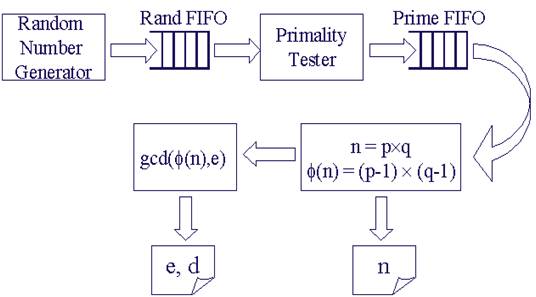
Figure 2. The System Architecture for RSA key generation
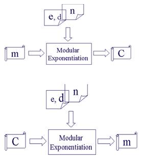
Figure 3. The RSA encryption/decryption structure
Anyone who needs to send a message to Bob can use n and e. For example, if Alice needs to send a message to Bob, she can change the message, usually a short one, to an integer. This is the plaintext. She then calculates the cipher text, using e and n.
C= Pe(mod n)
Alice sends C, the cipher text, to Bob.
Bob keeps φ and d private. When he receives the cipher text, he uses his private key d to decrypt the message:
P= Cd (mod n)
For RSA to work, the value of P must be less than the value of n. If P is a large number, the plaintext needs to be divided into blocks to make P less than n.
Choose p = 3 and q = 11
Compute n = p * q = 3 * 11 = 33
Compute φ(n) = (p - 1) * (q - 1) = 2 * 10 = 20
Choose e such that 1 < e < φ(n) and e and n are coprime.
Let e = 7
Compute a value for d such that (d * e) % φ (n) = 1.
One solution is d = 3 [(3 * 7) % 20 = 1]
Public key is (e, n) => (7, 33)
Private key is (d, n) => (3, 33)
The encryption of m = 2 is c = 27 % 33 = 29
The decryption of c = 29 is m = 293 % 33 = 2
[7]. This paper describes the implementation of RSA encryption/decryption algorithm on FPGA using 128 bits key size.
Input: A, B, n
Output: M = A*B mod n
P <= A;
M <= 0;
for i = 0 to k-1
if Bi = 1
M <= (M + P) mod n;
end if
P <= 2*P mod n;
end for
return M;
The modular exponentiation operation is simply an exponentiation operation where modular multiplication is intensively performed. They implemented the 512-bit and 1024-bit modular exponentiation components using LR binary method, where LR stands for the Left-to-Right scanning direction of the exponent. The following pseudo code describes the LR binary algorithm.
Input: A, B, n
Output: E = AB mod n
E <= 1;
for i = k-1 to 0
if Bi = 1
E <= A*E mod n;
end if
if i ≠ 0
After they get (n), we need to find a small number e with gcd (Ф(n),e) = 1, which indicates that e is relative prime to Ф(n) and its multiplicative inverse modulo Ф(n) exists. Extended Euclidean algorithm was implemented to find gcd (Ф(n),e), if the gcd is 1, e and its multiplicative inverse d are returned. The following pseudo code shows the extended Euclidean algorithm [6]. They simplified the algorithm by removing unnecessary variables and computations and made it more suitable for hardware implementation.
Extended Euclid (m,b)
 (A1, A2, A3) <= (1, 0, m);
(B1, B2, B3) <= (0, 1, b);
loop:
if B3 = 0
return
A3 = gcd(m,b);
end if
if B3 = 1
return B3 = gcd(m,b);
B2 = b-1 mod m;
end if
Q <= A3/B3;
(T1, T2, T3) <= (A1 - Q*B1, A2 - Q*B2, A3 - Q*B3);
(A1, A2, A3) <= (B1, B2, B3); (B1, B2, B3) <= (T1, T2, T3);
goto loop;
Simplified Extended Euclid (m,b)
start: (A2, A3) <= (0, m);
(B2, B3) <= (1, b);
loop: if B3 = 0
b <= fetch_new_b;
goto start;
end if
if B3 = 1
return (B3, B2);
end if
Q <= A3/B3; T3 <= A3 mod B3;
T2 <= A2 + Q*B2;
(A2, A3) <= (B2, B3); (B2, B3) <= (T2, T3);
goto loop;
E <= E*E mod n;
end if
end for
return E;
Linear Feedback Shift Register (LFSR) is used to generate the pseudo random numbers. In particular, Fibonacci LFSR was implemented because it is more suitable for hardware implementation than Galios LFSR. In theory, an n n-bit linear feedback shift register can generate a (2n - 1)- bit long pseudo random sequence before repeating. However, an LFSR with a maximal period must satisfy the following property: the polynomial formed from a tap sequence plus the constant 1 must be a primitive polynomial modulo 2 [3].. They are unable to find the primitive polynomial for a 512-bit LFSR, so they implemented a 521-bit LFSR and used its least significant 512 bits to generate 512-bit pseudo random numbers. The primitive polynomial for a 512 bit LFSR was obtained, which is x512 + x32 + 1. In order to get a 1024-bit n (n = q*p, where p, q are primes), they set the leading two bits of the random numbers to 1s, which ensures that the leading bit of n is always 1 (therefore n is 1024-bit number). Figure 4 shows the structure of the 521-bit LFSR, and the 512-bit random number generator implemented using the 521- bit LFSR.
To compute n and Ф(n) from p and q, regular multiplier is needed. They implemented a 1024-bit multiplier using the simple shift-add algorithm.
They used Xilinx Core Generator System to generate a 12- entry rand FIFO and a 12-entry prime FIFO.
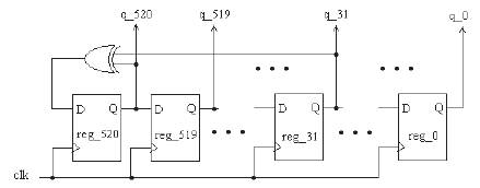
Figure 4. Structure of the 521-bit LFSR
LabVIEW (Laboratory Virtual Instrument Engineering Workbench), created by National Instruments (www.ni.com) is a graphical programming language that uses icons instead of lines of text to create applications. Lab VIEW programs/codes are called Virtual Instruments, or Vis for short. LabVIEW is used for Data acquisition, signal Processing (Analysis), and hardware control, It is a typical instrument configuration based on Lab view. LabVIEW is commonly used for data acquisition, instrument control, and industrial automation.
Figure 5 shows the Front Panel window of Encryption using Lab View and Figure 6 shows the Block Diagram window of Encryption using Lab View
Figure 7 shows the Front Panel window of decryption using Lab View and Figure 8 shows the Block Diagram window of Decryption using Lab View.
Figure 9 shows the Verilog Output for both encryption and decryption.
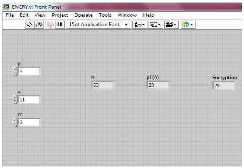
Figure 5. Front Panel window of Encryption using Lab View
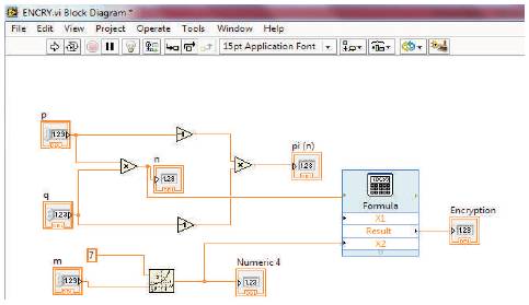
Figure 6. Block Diagram window of Encryption using Lab View
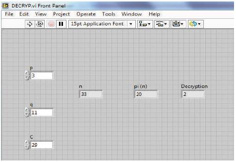
Figure 7. Front Panel window of decryption using Lab View
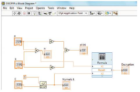
Figure 8. Block Diagram window of Decryption using Lab View
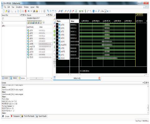
Figure 9. Verilog Output for both encryption and decryption
Although RSA can be used to encrypt and decrypt actual messages, it is very slow if the message is long. Therefore, it is useful for short messages such as a small message Digest or a symmetric key to be used for a symmetric-key cryptosystem. In particular, RSA is used in digital signatures and other cryptosystems that often need to encrypt a small message without having access to a symmetric key [5]. RSA is also used for authentication.
The Verilog and LabVIEW code for RSA Encryption/ Decryption algorithm is developed block wise. Optimized and Synthesizable Verilog code for each block is synthesized using Xilinx ISE 12.1 and verified to be functionally correct. The maximum clock frequency is found to be 101.061 MHz, since the device requires more than 100% resources, it is difficult to implement in FPGA.