[1]
The Z-source inverter is a relatively recent converter topology that exhibits both voltage-buck and voltage-boost capability. The Z-source concept can be applied to all dc-to-ac, ac-to-ac, ac-to-dc, and dc-to-dc power conversion whether two level or multilevel. Multilevel converters offer many benefits for high power applications. Z-source concept was extended to neutral point clamped inverter. The contribution of this paper is the digital implementation of SVM technique using 8-bit microcontroller for Z-source NPC. The proposed system uses 8-bit PIC 16F877A microcontroller to generate SVPWM (Space Vector Pulse Width Modulation) signal needed to trigger the gates of IGBT bridge of the multilevel inverter. This method has the benefits in terms of implementation and harmonic performance. By this method, the operation of Z-source arrangement can be optimized and implemented digitally without introducing any extra commutations.
Many industrial applications require higher power converters (inverters). Multilevel converters offer many benefits for higher power applications that include an ability to synthesize voltage waveforms with lower harmonic content than two-level converters and operation at higher dc voltages using series connection of a basic switching cell of one type or another [1], [2]. The most common multilevel topologies are cascaded with the inverter, the diode clamped inverter, and the capacitor clamped inverter. Among the three, the three level diode clamped [also known as the Neutral Point Clamped (NPC)] inverter has become popular in medium voltage drives [3].
The NPC inverter cannot produce an output line-to-line voltage greater than the dc source voltage. Z-source inverter topology was proposed to overcome the limitations of traditional inverters [4]. The Z-source concept was extended to the NPC inverter. This Z-source NPC inverter is expensive because it uses two Z-source networks, two isolated dc sources, and requires complex modulator for balancing the boosting of each Z-source network. To overcome the above limitations there is Reduced Wlement Count (REC) Z-source NPC inverter [5]. The modulation of the REC Z-source inverter using Space Vector Modulation (SVM) technique offers better harmonic performance and can more conveniently handle the overall switching patterns and the constraints and it is simple to be implemented using DSP [6].
The topology of two level Z-source concept is shown in Figure 1. The difference between Z-source inverter and a traditional Voltage Source Inverter (VSI) is the presence of Z-source network comprising a split inductor (L1 and L2 ) and two capacitors (C1 and C2 ). The unique feature of the two level Z-source inverter is that the output ac voltage fundamental can be controlled to any value between zero and infinity (regardless) of the dc source voltage. The Z-source multilevel inverter utilizes shoot-through state to boost the input dc voltage of inverter switches when both switches in the same phase leg are on. The Z- source inverters are having lower costs, reliability, less complexity and higher efficiency.
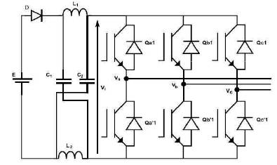
Figure 1. Topology of two level Z-source inverter
In traditional NPC inverter, if m is the number of output voltage level, then the number of capacitors required on the DC bus are (m-1), the number of power electronic switches per phase are 2(m-1) and the number of diodes per phase are 2(m-2).
Initially consider the operation of one phase leg of traditional NPC inverter as shown in Figure 2. The operation of each inverter phase leg can be represented by three switching states P, O, N. Switching state P denotes that the upper two switches in a phase leg are gated ON, N indicates that the lower two switches conduct, and O signifies that the inner two switches are gated ON.
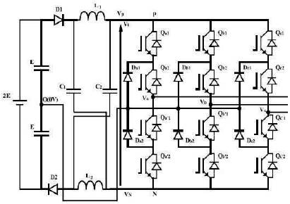
Figure 2. Topology of an REC Z-source NPC inverter
However, each phase leg of the Z-source NPC inverter has three extra switching states that resemble the “O” state of the traditional NPC inverter. These extra switching states occur when all the four switches in any phase leg are gated ON [Full-Shoot-Through (FST)], or the three upper switches in any phase leg are gated ON [Upper-Shoot- Through (UST)] or the three bottom switches in any phase leg are gated ON [Lower Shoot- Through (LST)]. These shoot-through states are forbidden in the traditional NPC inverter because they would cause a short circuit of the dc-side capacitors. Again, the Z-source network makes these shoot-through states permissible and provides the means for boost operation.
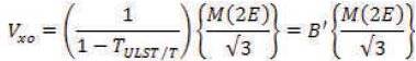
In Figure 2, the REC Z-source NPC inverter is supplied with a split dc source. The middle point O is taken as a reference. Switching states of REC Z-source NPC inverter is shown in Table 1. When the REC Z-source NPC inverter is operated without any shoot-through states, then Vi is equivalent to 2E. With this kind of operation, the maximum obtainable output line-to-line voltage cannot exceed line-to-line voltage greater than 2E, and shoot-through states are carefully inserted into selected phase legs to boost the input voltage to Vi > 2E before it is inverted by the NPC circuitry. Thus, the REC Z-source inverter can boost and buck the output lineto- line voltage with a single-stage structure.

Table 1. Switching states of an REC Z-source NPC inverter
The operation is using the FST and NST states, that is possible (termed the FST operating mode), but it is preferable to use the UST and LST states in the place of FST states (termed the ULST operating mode), because it produces an output voltage with enhanced waveform quality.
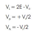
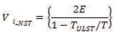
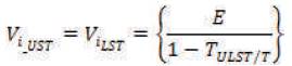
Assuming that the Z-source network is symmetrical (L1 =L2 =L and C1 =C2 =C), then VL1 =VL2 =VL and VC1 =VC2 =VC and the voltage expressions for NST, UST and LST are given as follows:
NST
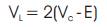
UST
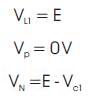
LST
By averaging the inductor voltage over one switching period,
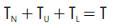
Where TN , TU , and TL are the duration of the NST, UST, and LST states respectively and T is the switching period.
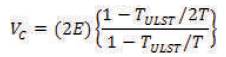
DC-link voltage during the NST, UST, LST states are given as
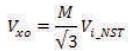
Fundamental peak ac output voltage VXO (xƐ {a, b, c}) is given by
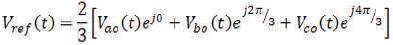
The space vector diagram for NPC inverter for sector 1 is shown in Figure 3. The reference vector Ṽref is given as
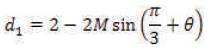
The reference vector is synthesized with three nearest space vectors. If it is located in triangle 3, the nearest three vectors are Ṽ1 , Ṽ7 , and Ṽ13 . The duty ratios for these vectors are given as
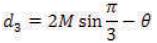
To complete the modulation process, the selected voltage vectors are applied according to a switching sequence. Seven segment switching sequence is adopted in SVM as shown in Table 2.
Figure 3. Space vector diagram of sector 1 for a three-level inverter
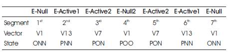
Table 2. Seven-segment switching sequence in triangle3
It is necessary to determine where the UST and LST states can be inserted; a shoot through state can be introduced on any phase which is switched to the zero (O) level without affecting that phase leg. The permissible shoot through states are shown in Table 3.
A modified switching sequence can achieve voltage boosting in an optimal way as follows. Seven segment switching sequence for traditional NPC and an REC Zsource NPC is given in Figure 4.
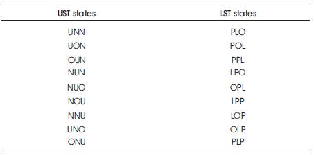
Table 3. Permissible UST and LST states
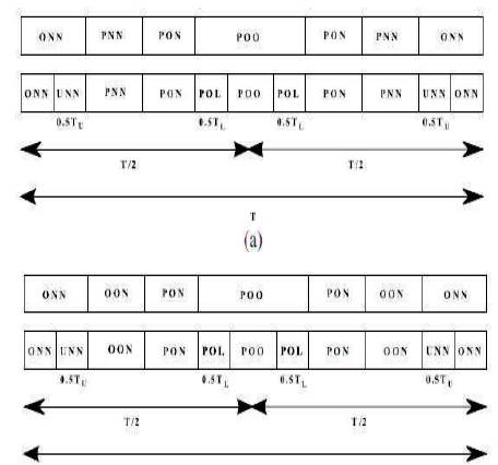
Figure 4. Modulation of traditional NPC and Z-source NPC when the reference vector is in (a) triangle 3 and (b) triangle 2a on the three level vector diagram shown in the Figure 3
The switching sequence for various triangles of sector 1 is shown in Table 4.
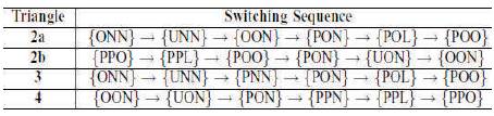
Table 4. Switching sequences and insertion of shoot-through states in triangle 2-4
The algorithm of SVPWM could be summarized in the following two main steps
Step 1: Determination of space vectors and angle (θ ).
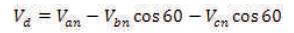
The first step is to determine Vd, Vq, Vref and angle ( θ) through the following equations which use abc to dq Park transformation as shown in Figure 4:
Where fs = fundamental frequency
Step 2: Determination of time duration.
Second step is to determine the time durations: T1 , T2 and T0 for the first adjacent vector, second adjacent vector and zero-vector V1 , V2 and Vo respectively. The vector summation of adjacent vectors gives the reference voltage vector Vref.
The following lines describe the implementation of SVPWM in the digital domain (i.e. PIC micro controller). PIC microcontroller consists of several input/output pins that used for transmitting or receiving signals from the connected peripheral. Six of these pins could be used for the generated PWM output signals to drive the MOSFETs of Z-source neutral point clamped inverter.
For digital implementation, the following quantities should be known before applying SVPWM algorithm to PIC to approximate the position of VS.
This module reads the values of the desired (fundamental) frequency, then it generates the appropriate PWM signals using space algorithm. This process could be summarized using in Program Description Language (PDL) as follows:
Begin
Set initial values
Read fundamental frequency
Calculate step value
1 Sector = 1
2 Find T and T from look-up table
TZ = TS – TA – TB
Send switching pattern of current sector with delay times to port B and T
Sector = Sector +1 (T );
If sector>6 then goto 1 else goto
End
As discussed earlier, PIC16F877A microcontroller was used for the implementation of SVPWM algorithm. The software that was used for PIC micro controller programming was MikroC compiler, while WinPIC800 software was used for downloading the program into the PIC micro controller. The process of micro controller programming could be summarized in the following steps:
First step of micro controller programming is writing the algorithm of the objective program. Second step is writing the C code based on program algorithm. Compiling C code is the third step to verify the written code and then doing required corrections or modifications. Compilation process generates the several types of files such as C-type and Hex- type. The C-type file contains the text code of the program which could be edited and compiled later. The Hex-type file contains the program instructions in Hexadecimal format which suits the micro controller. In the next step, PIC is applied to JDM programmer, while WinPIC800 software is used to download the Hexadecimal file into PIC through RS-232 serial port of PC
There are 12 IGBT bridges in the inverter. Hence 12 driver units are required. For simplicity single unit is shown in Figure 5. The proposed techniques are stored in the micro controller, which generates the gate pulses, which are then given to the driver unit.
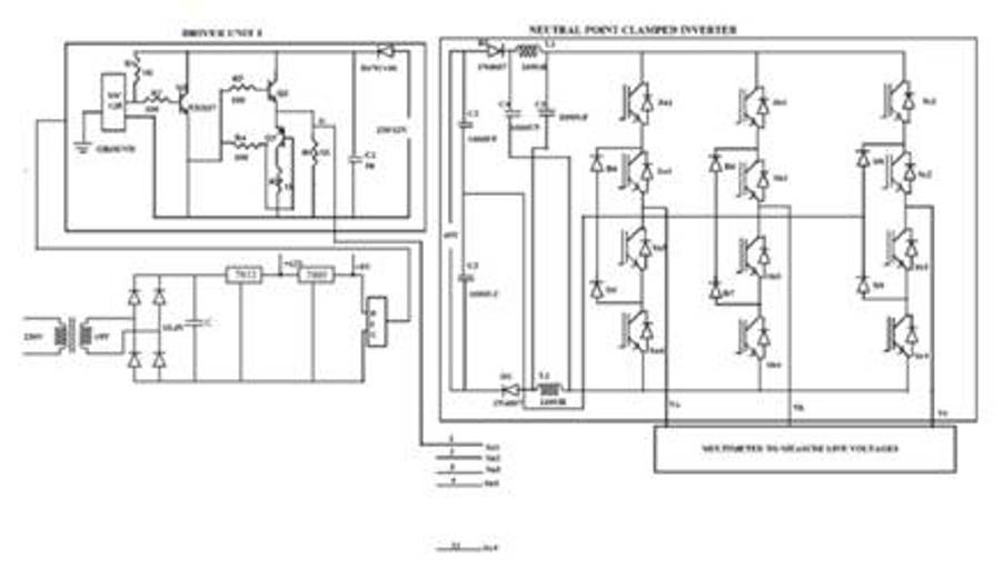
Figure 5. Laboratory work of the proposed system
The output waveforms from an REC Z-source NPC inverter is given in Figure 6. The modulation index is 0.825 and boost factor is 0.35. When the boost factor is other than 1, then the output voltage is boosted, otherwise output voltage is reduced, and that depends on the modulation index.
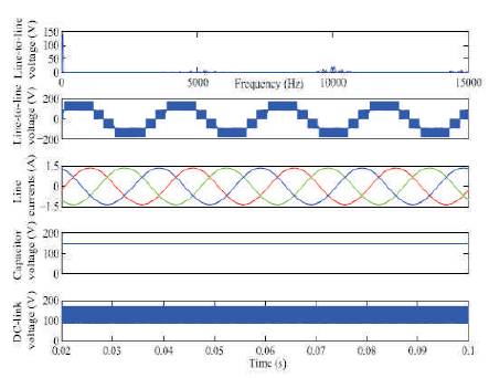
Figure 6. Waveforms obtained from the REC Z-Source NPC Inverter (Top to Bottom) Waveforms of line to line voltage, line current, capacitor voltage and dc link voltage for M=0.825, TULST/T=0.35
This paper describes the digital implementation of SVPWM technique for Z-source neutral point clamped inverter. The proposed system uses 8-bit PIC16F877A micro controller for generating SVPWM signal that is needed to trigger the gates of IGBT bridge of the inverter. This inverter contains low-pass LC-filter to produce a sine waveform output. The experimental results show that the ability of the proposed system to generate a three-phase sine wave signal with desired frequency.