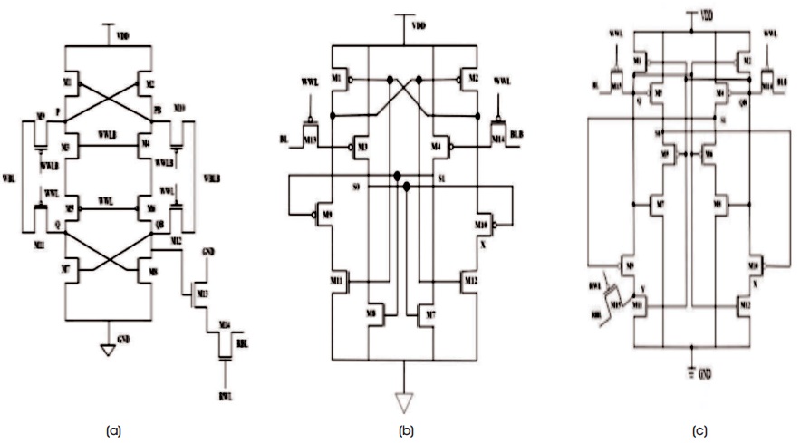
Figure 1. Schematic Diagram Existing SRAM Cells a) ILS 14T b) RHBD 12T and c) RHBD 15T
This paper presents low power radiation hardened cells. In this paper, two designs are proposed namely Interleaving Stacked Cell 12T (ILS 12T) and Radiation Hardened by Design 14T (RHBD 14T) SRAM cell design, in order to make the cell tolerant to single event upset and partially tolerant to double node upset. The new designed SRAM cell is ineffective to both 0-1 and 1-0 upset. The simulation software Cadence Virtuoso simulation tool is employed and it analysed a reduction in power.
Increase of VLSI applications demands for portable device size and battery operated embedded systems with greater scale. Low-power random access memory (RAM) is a viable technology for meeting the growing demand for massive data storages that must be faster than current technologies. Typically, SRAM is most preferred because of its low power consumption and high speed.
Static random access memory (SRAM) is susceptible to the high energy particles under harsh radiation environments. Sensitive storage nodes in SRAM cells can be flipped by collecting sufficient free charges or latching the single event transient from logic circuits. The error in the device output or operation caused as a result of the strike is called a soft error or single event upset.
Recent days there are many radiations hardened designs proposed to overcome the effect of single event upset.
Low power SRAM cell designs have been analyzed for power consumption, write delay. Here gated VDD and MTCMOS design techniques have been employed to reduce the power consumed by the SRAM cell with a trade off in area overhead (Bhaskar, 2017).
SRAM fabrication using dual and triple well were implemented at 28-nm technology. This triple well found better for reduced voltages with reduced soft error (Narasimham et al., 2015).
A 10T soft error robust SRAM cell is compatible with standard CMOS process and gives differential read operation. The cell is known as “Quatro-10T” cell and accelerated by neutron radiation implementing a 32-kB SRAM macro in 90- nm CMOS technology. This has efficient area with less leakage but read and write operations are slow (Jahinuzzaman et al., 2009).
There are two types of a soft error hardened 10T SRAM cells with high static noise margin for low voltage operation. Area overhead NMOS stacked with 10T cell has read SNM and high soft error silence (Jung et al., 2012).
SRAM cells namely RHD11 and RHD13 has higher robustness against single event multiple effects with less layout area and higher write delay (Rajaei et al., 2015).
The radiation hardened SRAM bit cell is targeted at lowvoltage performance while having high soft error robustness. The 13T dual-driven separated-feedback bit cell uses many techniques to achieve robust SEU suppression with scaled supply voltages and high-radiation tolerance with larger layout area (Atias et al., 2016).
A comparison about various structures of SRAM cell compute various parameters to improve the performance of the SRAM cell like SNM, delay but there is issue of trade off with speed and area (Singariya & Mishra, 2014).
With area overhead, a SEU-tolerant latch based on Quatro and NMOS feedback transistors has a greater upset LET threshold and lower cross-section with reduced SEU (Wang et al., 2014).
For typical strikes, an action approach of heavy-ion data from a 130-nm bulk CMOS process utilising a common single-event charge collection reduces the single event pulse, but for angled strikes, the single event pulse increases.
A radiation hardened by design memory cell (RHD 12T) with 12 transistors in 65-nm CMOS technology that is highly reliable. Because of charge sharing, this design has been able to tolerate single event upset with multi node upset in a single memory cell. When area, power usage, and access time are taken into consideration, performance improves (Qi et al., 2016).
A radiation hardened by design 12T memory cell can withstand single node and multi node upsets based on upset physical processes, however it has a longer read access time, which is significant in space applications (Guo et al., 2014).
A radiation hardened 14T SRAM cell in 65 nm technology can give speed and power optimization and is ineffective to both single event upset and single event multi node with tradeoff in area overhead (Peng et al., 2018).
With a scalable area overhead voltage, a RHBD 15T SRAM cell design can endure single event double upset tolerance (SEDU). The 14T SRAM with a peripheral circuit designed in 28 nm technology can withstand the upset by preventing it from spreading to adjacent nodes and acting as radiation-hardened cells. However, there is a problem with overhead space and power (Han et al., 2020).
Various methodologies of SRAM cell have been used to reduce single event upset in SRAM and obtain low power but there is tradeoff between area and power. Hence, this work focuses on SRAM cell design to reduce single event upset with low power. Figure 1 shows the schematic diagram of existing SRAM cells.
Figure 1. Schematic Diagram Existing SRAM Cells a) ILS 14T b) RHBD 12T and c) RHBD 15T
The ILS 12T SRAM design and RHBD 12T has proposed in this paper. Figure 2 shows the diagram of proposed SRAM cells. ILS 12T comprises of 12 transistors (6 pMOS and 6 nMOS). Here, transistors M9-M12 are controlled by written word lines. Q, QB, P, PB are the storage nodes. The transistors M3- M6 are stacked transistors which improves the SEU immunity of 14T cell. Transistors M1, M2, M9 and M10 are connected with high threshold. Three stages of operation takes place in SRAM cells for write, read and hold.

Figure 2. Schematic of Proposed SRAM Cells a) ILS 12T and b) RHBD 14T
The information is written to the storages nodes, and when WWL is high, during that period transistors M9-M12 are on and the stacked transistors are at off state.
When the transistors M9-M12 are at off state, hold operation takes place. Read operation takes place with transistors M9-M12 which is in on state and the read operation takes place by storing the storage nodes. Q and P stores 0 and QB and PB stores 1.
When the bit line is high, information is written into storage nodes, and when it is low, the read operation occurs by storing the storage nodes. Q and S1 stores as “1” and storage nodes QB and S0 stores as “0”.
ILS 12t has an improved immunity of SEU tolerant with scalable Vdd.
When state change occurs at node Q due to any radiation, only the transistors M8 gets off and the rest of the nodes are unchanged. Similarly, when it changes from 1 to 0 only M7 gets off and cannot move to further nodes. Thus any radiations at this node will not affect the circuit.
When state change occurs at node QB, only the transistors M7 gets on and the rest of the nodes are unchanged. Similarly, when it is changed from 1 to 0 only M7 gets on and cannot move to further nodes.
When there is state change occuring at node P, only the transistors M1 gets off and the rest of the nodes are unchanged. Similarly when it is changed from 1 to 0 only M2 gets off and cannot move to further nodes.
When there is state change occuring at node Q only the transistors M1 gets off and the rest of the nodes are unchanged. Similarly when it is changed from 1 to 0 only M2 gets off and cannot move to further nodes.
The physical mechanism of upset in the proposed RHBD 14T remains intact and stores as “1", based on the physical mechanism of upset as Q is connected to the drain of the PMOS, which is in the off state. As a result, Q does not change and is unaffected by upset.
When there is a state change occuring at node QN from 0 to 1, transistors M4 and M1 gets off. So, Q remains unchanged, S1and S0 remains unchanged as transistors M9, M5 and M7, M11 gets off and on state. Finally, when transistors M6 and M12 gets on by the nodes Q and S0, QN returns to its original state “0”.
When a state change occurs at node S0 from 0 to 1, transistors M6 and M8 gets off and M10 gets on. So, S1 remains unchanged, and QN remains unchanged as transistors M12 and M6 gets on and off state. Finally, when transistors M9 and M7 gets on, S0 returns backs to its original state “0”.
When a state change occurs at node S1 from 1 to 0, due to the state change only transistors M9 and M7 gets off and on. So, S0 remain unchanged and long as in 0, QN remains unchanged by the nodes Q and S0 which makes the transistors M12 and M6 gets into on state. Finally, when transistors M4 gets on by the nodes QN, S1 returns back to its original state “1”.
Thus any radiations effect at any node will not affect the operation of the circuit.
Double node upset tolerance in the proposed ILS 12T and RHBD 14T are as follows:
Initially there is value of Q=1, QB=0, P=1 and PB=0 which is stored by the storage nodes respectively. Consider if a state change occurs at node Q (1-0) and QB (0-1), then only the transistors M8 and M7 gets off and on and the rest of the transistors remains unchanged. Simultaneously, the same process takes place in all the nodes and the simulation shows that there is partial upset tolerance to double node upset.
Initially the storage nodes have Q=1, QN=1, S1=1, S0=0. For a multi node upset, consider if there is a state change occuring at the storage nodes QN (0-1) and S0 (1-0), then the transistors M1, M7 and M4 is in off and transistors M9 is in on. When the transistors M5 and M11 gets on, there is chance for state change at node Q, but as per physical mechanism the node Q is connected to off PMOS drain and it stores “1”, it remained unchanged. Hence the transistors M3 is in off state, the node S0 remains unchanged and transistors M12 and M6 gets on and enable the QN node to return to its original state 0. As the node QN stores back its original value “0” so the transistors M4 gets on and makes the node S1 to store “1” which is the original state of node S1.
The overall upset tolerant analysis shows that the proposed SRAM cells are fully tolerant to single event upset and partially tolerant to double node upset.
Various radiation hardened SRAM cells such as ILS 14T, RHBD 12T and 15T are simulated and analysed using Cadence Virtuoso simulation tool. Figure 3 explains the read and write operations in ILS 12T and RHBD 14T.
In ILS 12T and RHBD 14T, bit lines and its complement of bit lines and write lines are the inputs. In ILS 12T the storage nodes such as Q, QB, and PB are the outputs. In RHBD 14T, the storage nodes such as Q, QB, S0 and S1 are the outputs as depicted in Figure 4.
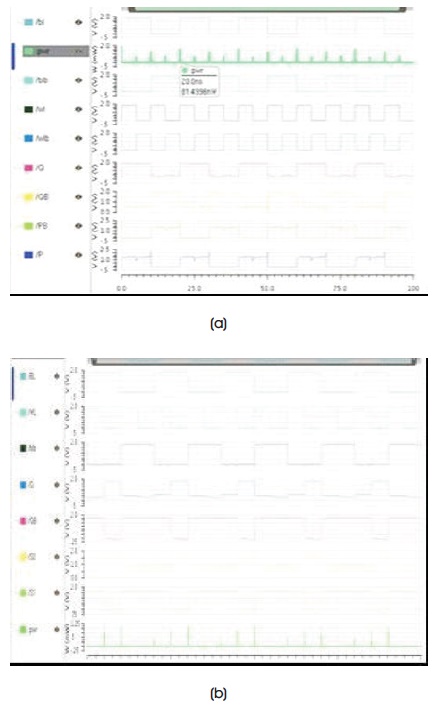
Figure 3. Output Waveform for Read and Operations of a) ILS 12T b) RHBD 14T
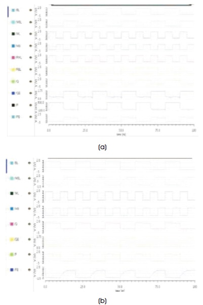
Figure 4. Sample Output Waveform of Upset Occurs at (a) Nodes QB (b) PB in ILS 12T
Interleaving stacked 12T SRAM cell design has a state change at nodes QB and PB. Due to the radiation effects there is no state occuring at the output nodes during read and write operations. The affected nodes do not affect other storage nodes in the circuit and return to its original state. The sample output waveform of upset occuring at ILS 12T and RHBD 14T is shown in Figure 5.
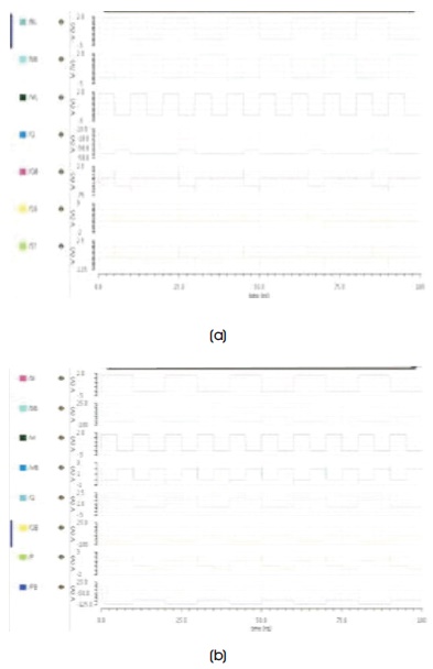
Figure 5. Sample Output Waveform of Upset Occurs at a) ILS 12T b) RHBD 14T
In this the proposed SRAM cell designed as ILS 12T and RHBD 14T have implemented and exhibit a power of 15.51 μW and 8.64 μW. The power consumption of proposed cells is less compared to other radiation hardened SRAM cells as in Table 1.
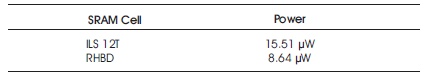
Table 1. Power Consumption of SRAM Cells
Simulation analysis shows that, the proposed ILS 12T and RHBD 14T SRAM cell can tolerate single event upset by the use of cadence virtuoso simulation tool. They are employed this to show that there is variation in power from microwatt to watt and there is reduced delay and area overhead. Table 2 explains the power consumption of various radiation hardened cells such as ILS 14T, RHBD 12T, RHBD 15T with ILS 12T and RHBD 14T with reduction in power.
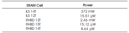
Table 2. Power Consumption of Various Radiation Hardened SRAM Cells
The proposed ILS 12T and RHBD 14T SRAM cell design are ineffective to single event upset and single event double node upset. Compared with ILS 14T, RHBD 12T, RSP 14T and RHBD 15T, the proposed hardened cells have less power consumption with improved speed in read and write access time. This enables to make a proposed cell suitable for low power applications.