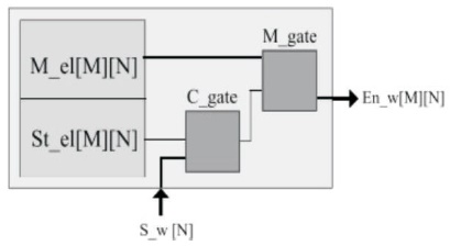
Figure 1. Single G-AETCAM (Irfan, & Ullah, 2017)
This paper presents a design for Gate-based ternary content-addressable memory (G-TCAM), utilizing G-AETCAM cells, which yields the location of given input information. The G-AETCAM cells utilizes flip-flop as memory component and control rationale hardware comprising of rationale entryways. One G-AETCAM cell encodes the input and put away the output into one encoded bit which brings about a match-line subsequent to passing from the input. G-AETCAM architecture is area efficient in terms of transistor count and speed of operations is high than the available TCAM architectures. The cascaded G-AETCAM cells are divided as banks, by considering each row as single bank of whole memory. The decoder logic used for memory design is modified by using reversible logic gate technique. Here, HL gate has been used instead of Line Decoder.
In today's life, we need high-performance memory for network system. Content-Addressable Memory is mainly used in search operation. Random Access Memory (RAM) performs lookups using a memory address which then returns the data from the address. CAM lookups do the opposite which returns the address of given input data word. A function calls the CAM by passing a key that consists of data word structure and the CAM lookup returns memory addresses, which is classified into two types, Binary CAM and Ternary CAM memory. Binary CAM is used for logic bits 0's and 1's, whereas TCAM deals with third bit X (called Don't Care (DC) bit or redundant bit) by the name Ternary. Applications of TCAM are mainly used in networking, i.e, Packet For warding, Packet Classification and Routers. The modern FPGAs have no TCAM memory, which can be implemented in either two ways, by RAM based TCAM and other is Logic based TCAM.
G-AETCAM cell is made up of a Masking Element (M_el), a Storage Element (St_el), a Comparison gate (C_gate) and a Masking gate (M_gate). M_el stores the masking bit which could be '1' or '0' depending on the virtual TCAM bit to be stored from conventional TCAM. If the virtual bit is '1' or '0', '0' will be stored in M_el. C_gate is an XNOR gate which compares the bit value stored in St_el and the input bit from the Search word (S_w[N]). M_gate is an OR gate which takes the bit value stored in M_el and output from C_gate as input and gives Nth bit of the Encoded word (En_w[M][N]) as output (Irfan, & Ullah, 2017). A single G-AETCAM cell is shown in Figure 1.
Figure 1. Single G-AETCAM (Irfan, & Ullah, 2017)
One G-AETCAM cell encodes the input and stored bit into one encoded bit which results in a match-line after passing from the AND-gate-array. It uses flip-flop as a memory element and a control logic circuitry consisting of logic gates.
A 4×4 G-AETCAM architecture with 16 G-AETCAM cells having four rows and four columns is shown in Figure 2. AND-gate-array consists of four 4-input AND gates. The output from the four G-AETCAM cells in a single row is fed to the corresponding AND gate of the AND-gate-array which gives a match-line (M_L) as output. When a 4-bit S_w is given at the input, first bit (S_w[1]) will be given as input to all of the G-AETCAM cells in first column, second (S_w[2]) in second, third (S_w[3]) in third, and fourth bit (S_w[4]) will be given as input to all of the GAETCAM cells in fourth column of the G-AETCAM matrix. A match-line results from the bitwise ANDing of all four bits (En_w[M][1], En_w[M][2], En_w[M][3] and En_w[M][4]) of the Mth Encoded word (En_w[M]). One match-line (M_L[M]) represents a MATCH or MISMATCH of the search word with the corresponding row or ultimately with the corresponding stored word. M varies from 1 to 4 in this case. M_L[1] represents match-line for the first row, M_L[2] represents match-line for the second row, M_L[3] represents match-line for the third row and M_L[4] represents match-line for the fourth row of the G-AETCAM memory (Irfan, & Ullah, 2017). These four match-lines serve as INPUT to the priority encoder.
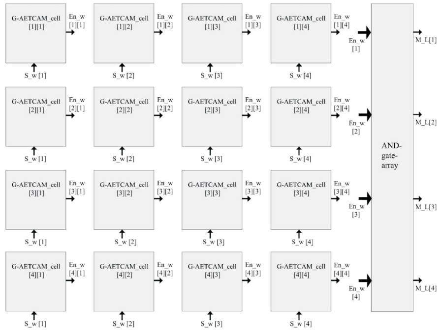
Figure 2. Cascaded (4 x 4 array) G-AETCAM Cells (Irfan, & Ullah, 2017)
By using the HL gate, all circuits will be designed with low Quantum Cost, less number of content inputs and Garbage Outputs. Figure 3 shows a HL reversible logic gates. This kind of design saves power and minimizes the amount of dissipated heat energy. A circuit designed with solitary reversible logic gates is known a reversible logic circuit and it gives no power dissipation. A reversible logic gate is defined as a N x N logic gate with equal number of input and output terminals and one to one mapping among input and output bit streams. To maintain reversibility, it is necessary to apply some extra inputs as logic 0/1 are known as constant inputs (K.Is) and also a reversible logic gate generates annoying outputs (unemployed outputs) are known as garbage outputs (G.Os). A reversible logic circuit performance will be measured in terms of Quantum Cost (Reddy et al., 2018).
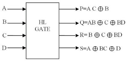
Figure 3. HL Reversible Logic Gate (Reddy et al., 2018)
Decoders are the prime elements to select the memory devices and for instruction decoding. Thus reversible decoders are developed with different reversible logic gates. The Figure 4 represents the decoder logic using one to one mapping among input and output bit streams. 2:4 decoder using a single gate known as HL gate with 2- inputs (K.Is) and, no Garbage outputs (G.Os) and Quantum Cost (Q.C) is 7. The inputs other than A, B are constant to balance the input signals and reduce Garbage Outputs.
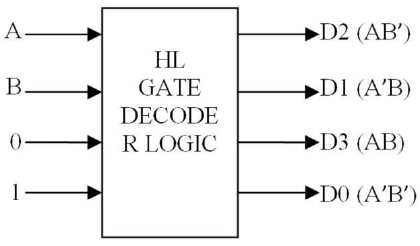
Figure 4. 2:4 Decoder with HL Gate (Reddy et al., 2018)
Irfan et al. (2020) have proposed a method of RPE-TCAM. This paper presents TCAM cell that employs flipflops as storage element. The circuit requires two flipflops for read, write and search operation for TCAM. Advantage is reduced power dissipation, reduced transistor count and search/match operation performance. The disadvantage is that this proposed method encountered stability issues.
Ullah et al. (2015) have proposed a method using SRAM based TCAM and hybrid partitioning. For further improvement in performance UE-TCAM is used. Advantage is reducing latency, also reduces memory requirement and also reduce power consumption and improves speed. The disadvantage is that the implementation is expensive and also it adds complexity to the TCAM architecture.
Junsangsri et al. (2015) have proposed a novel design of Phase Change Memory (PCM) as storage element and one CMOS transistor as control element. A memory core consists of CMOS transistor and a PCM for search operation, the data in the memory core and the value is established using two differential sense amplifiers. Advantage is significant advantages in terms of write time, search time, power consumption and reduced transistor count. Utilization of TCAM comes at the cost of increased area and power consumption are its disadvantages.
Irfan and Ullah (2017) have proposed a method of a matrix of G-AETCAM cells arranged in the form of rows and columns using flip-flop as memory element and control logic circuit. The advantage of this method is the reduction in the area and increase in the speed of operations. The disadvantage is that there exists a delay between the elements.
Syed et al. (2017) have proposed a method for update module implementation and hybrid partitioning. Update module is used for replacing the old TCAM contents with fresh contents. Advantage is it improves memory access speed, scalability, cost and storage density. The disadvantage is the trade-off between worst case latency and memory resources.
Hellkamp and Nepal (2018) have proposed a method of using (CNTFET) Carbon Nanotube Based Transistors. In this paper, silicon based transistors are replaced by carbon nanotube based transistors which is similar to MOS transistors. It can be formed by using doped carbon nanotubes to move majority carriers from drain to source under the influence of electric field applied to the gate. Advantage is reduced transistor count upto 31% and the disadvantage is match line leakage and cell stability.
Ahmed et al. (2016) have proposed a novel design in resource-efficient SRAM based TCAM (REST), which emulates TCAM functionality using optimal resources. SRAM unit is divided into multiple virtual blocks to store the address information presented in the TCAM table. Advantage is the increase in address space of SRAM unit, TCAM bits and reduces cost. Disadvantage is increase in the number of transistor when compared to SRAM and less storage efficiency.
Irfan et al. (2019) have proposed a method based on the lookup tables (LUTs) and partial reconfiguration to achieve more effective use of the FPGA resource, the proposed method results to show achievement in resource usage. The advantage is it provides the flexibility to modify the designs once deployed. Disadvantage is TCAM implemented in networking application such as packet classification is more complex than normal memories. Hence, TCAMs are emulated with logic resources inside FPGA.
Irfan et al. (2019) have proposed a novel method of TCAM architecture based on Distributed RAM based TCAM (DTCAM) using a building block. And also exploiting LUTs-FF i.e. LUTS-Flipflops pair nature of Xilinx FPGAs. The advantage is, improved throughput of the TCAM architecture and reduced hardware utilization. Disadvantage is the lack of efficient utilization hardware resources.
Ullah et al. (2019) have proposed a novel method using distributed RAM with quad-ports in FPGAs. More specifically, lookup tables RAMs (LUTRAMs) available in resource are configured as quadport RAM which constitutes the basic memory (BM) in the implementation of DURE. Advantage is single-cycle search latency and higher performance per area and the disadvantage is higher latency.
Karam et al. (2015) have proposed a method emerging challenges and opportunities in implementing different varieties of CAM and associative memory structures. This paper describes the circuit level implementations using CMOS-silicon and non-silicon memory technologies. Advantage is the use of CMOS and non CMOS brings low power and higher speed parallel search capabilities. The widespread applications are in many domains such as cache controls in processors, look up tables in high speed routers.
Ullah et al. (2018) have proposed a novel method in pre classifier based architecture for EE-TCAM as it divides TCAM into several sub tables of balanced sizes. The proposed architecture selectively activates particular SRAM blocks for each incoming search word. Advantage is that the architecture achieves power consumption of least three times than existing and also gives higher performance.
Various techniques has been implemented for TCAM memory and G-TCAM architectures.
TCAM implementation using 16-T transistors is limited to area and power efficiency and high cost. Hence to overcome this limitations cascading of G-TCAM cells in a array of matrix has been simulated to reduce hardware complexity and improve area and power efficiency
The proposed G-AETCAM is simulated using Xilinx Vivado Design Suite version 2018.
The search operation of one G-TCAM cell is simulated and the results are discussed. The schematic shown in Figure 5 is simulated output of G-TCAM cell. The input to the memory is taken from clock gating circuit and the output of TCAM memory is compared using 2-Bit comparator and then output is passed to priority encoder which gives final output of memory called Match line (ML). The search operation of single cell is performed by XNOR Logic.
The bank selection of cascaded G-TCAM is implemented using Xilinx Vivado. Only one bank is selected based on the input search key, the remaining are in ideal mode for power consumption. Here, memory is divided into four banks and the simulated output is shown below in Figure 6.
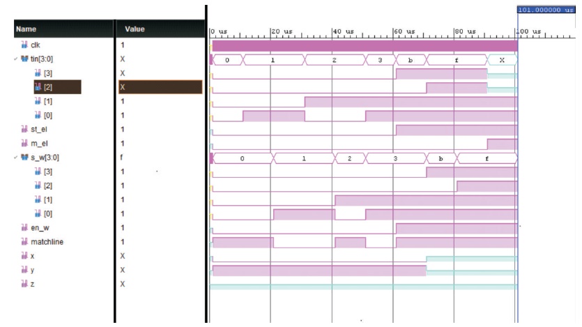
Figure 5. Simulated Result of Single G-TCAM Cell
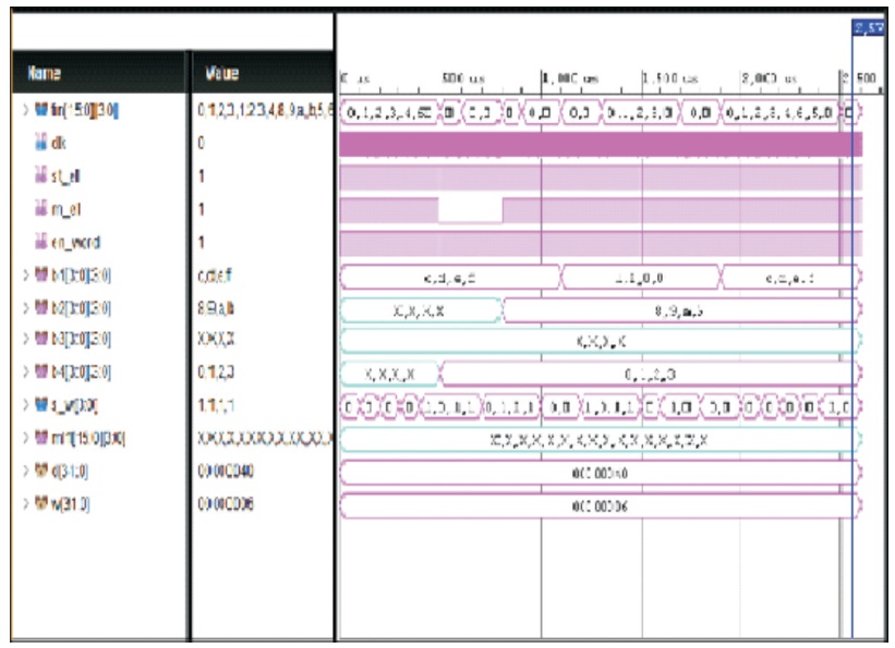
Figure 6. Simulated Result of Bank Selection of G-TCAM Cell
The power of single G-TCAM cell is estimated using Quatus Tool. The power value is estimated for search operation of single G-TCAM cell as shown in Figure 7.
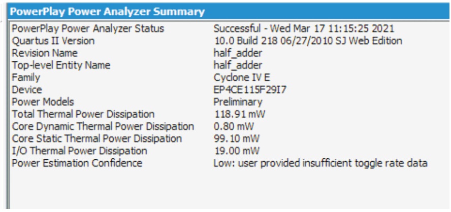
Figure 7. Power Estimated for Single G-TCAM Cell
G-TCAM based memory architecture has been proposed by flip-flops and logic gates.
Hardware reduction is achieved by comparing with TCAM with 16-T Transistors and also power reduction is achieved. Cascaded architecture is implemented by combining GTCAM cells in a 4 x 4 matrix. The implementation of cascading of basic TCAM is a complex design which consumes large area and increase power consumption and cost of the system. The whole memory is divided into four banks and the decoder logic is used with Reversible logic gate (HL gate).
In future, the cascade memory architecture would be designed for fast searching applications and storing applications of data in FPGAs for real time using artificial intelligence.