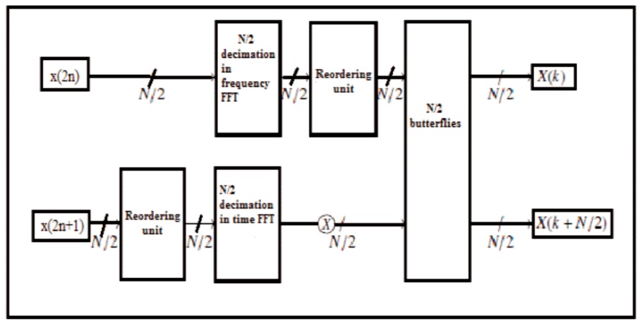
Figure 1. Idea to Implement the Proposed Method (Glittas, 2016)
The fundamental operation in digital signal processing and wireless signal processing applications like Multiple Input and Multiple Output (MIMO), Orthogonal Frequency Division Multiple Access (OFDM) is a Fast Fourier Transform(FFT). FFT is the fastest way of computing Discrete Fourier Transform by way of Divide and Conquer technique. There are different ways of developing VLSI architecture for FFT processor by using Delay elements (SDF, MDF), Delay Commutators (SDC, MDC). The famous architecture for FFT processor is Single Delay Feedback (SDF) architecture which has an advantage of full (100%) hardware utilization. Another famous architecture known as Multipath Delay Commutator (MDC) has an advantage high throughput at 50% of hardware utilization. In this project, we propose VLSI hardware architecture for twin data stream processing using Radix-2 algorithm. The proposed architecture is based on pipelined MDC architecture. The proposed architecture uses both Decimation-In-Time FFT (DIT-FFT) and Decimation-In-Frequency FFT (DIF-FFT) to process even and odd samples of twin data streams. In this architecture the bit reversal operation is carried out by the proposed architecture itself. When compare to other exiting architecture to proposed work designed with shift registers, bit reverserval operation performed in FFT with a high throughput and less numbers of registers.
The design of the pipeline FFT processor architecture was the subject of intense research in the 1970s, when realtime processing was required for applications such as radar signal processing, long before VLSI technology passed to the integration level of the system. Since then, several architectures have been proposed in the last 20 years, and interest in technology has grown and advanced. Here we develop a new architecture with a bibliographic survey of several references. Here, the additive butterfly is separated from the multiplier to clearly indicate the hardware requirements, and the control mechanisms and turn factor reading are omitted for clarity in each document.
FFT is widely used in wireless communication, with major applications in OFDM, ultra-wide band, terrestrial digital video transmission and digital signal processing. Several researchers have proposed several VLSI architectures to achieve a low area, low power and high performance.
He and Torkelson (1998) proposed a radix-22 hardwareoriented algorithm. Although it has a radix-4 multiplication complexity, the radix-2 butterfly structure is preserved in SFG. Based on this algorithm, a new efficient channeled FFT architecture, the R22SDF architecture, has been proposed. Single route delay (SDF) feedback and the multipath delay switch (MDC) are very common and describe a family of channeled FFT architectures (He & Torkelson, 1998). The applications need to process multiple data streams. Therefore, we need to run multiple FFTs at the same time, and we also need an obsessed bit investment circuit to get the output in an extremely powerful creation. Lin et al. (2006) proposed a replacement of the DVFS FFT processor for optimal performance and low-power OFDM MIMO systems. With the planned MDF design and the OLVDS theme, the FFT method will process one to eight transmissions of three hundred M samples from a pair of 56 FFT or 2.4 G sample/s of 256 FFT points with minimum voltage/frequency. Compared to normal technique, the typical power reduction with the planned DVFS FFT style is the 39th, 31st, and 19th separately in the FF, TT, and SS corners. FFT design can process multiple independent information flows. However, all information flows from the area unit are processed by an FFT processor (Lin et al., 2006). If eight information flows are processed in 2 domains, then the output of multiple information flows cannot be used in parallel. To process information simultaneously multiple FFT processors are required. Cho and Kang (2010) proposed the WPAN multimode FFT processor for personal wireless space networks, wireless native space networks (WLANs), and metropolitan space network (WMAN) wireless applications. The versatile multipath delay feedback (FRCMDF) design enables the costeffective execution of variable-length/multi-flow FFT hardware that can have high performance.
Wireless local area network applications are processed in one to four data streams, however, there is no specific bit inversion circuit. In Peng et al. (2010), a reconfigurable architecture to achieve high performance was proposed. This architecture handles a flow of 2048 FFT points, up to 2 flows of 1024 FFT points, or up to 4 flows of 512 FFT points. The architecture consists of a modified FFT single delay feedback (SDF) FFT. The sampling rate of the system varies with the length of FFT. Matchless clock lock technology is used to reduce energy consumption. Data from different data streams are intertwined for simultaneous processing The architecture of does not have a specific bit inversion circuit. Jiang (2007) proposed an orthogonal frequency division multiplexing system (MIMO-OFDM) processor of variable length of Fourier multiple transformations (FFT) of variable length and multiple-input. In general, multiple streams are handled by multi independent data streams.
A bus processed one to four streams of data. Multiple knowledge methods for native wireless network applications. However, there is no specific bit of investment circuit. Peng et al. (2010), proposed a reconfigurable design for high performance. This design handled a flow of 2048 FFT points, up to a pair of flows of 1024 FFT points, or up to four flows of 512 FFT points. The design consists of a modified single delay feedback FFT (SDF). System speed varies with FFT length. Clock lock technology without latch is used to reduce power consumption. Jiang (2007) proposed the Orthogonal Frequency Divider Multiplexing System (MIMO-OFDM) variable-length multiple transformation Fourier (FFT) variable-length multiple input system.
Information flows in a square signal processed by a FFT processor contains four independent information flow, procesed one by one. Cooley and Tukey (1965) presented mathematical framework for a Fourier (FFT) rework processor that will generate traditional output order sequences.
Specific circuits are planned to rearrange FFT outputs in a very traditional order. As a result, the circuits are integrated into the FFT design, reducing the general style log requirements from 5N / a pair to 2N frequency.
This distinctive flow design needs process 2 or many streams and needs 2 or many similar architectures in parallel. The full range of records (including record organization) required for the FFT processor is 2N or many (Cooley & Tukey, 1965). The design needs fewer summers compared to the planned design. Its performance is lower than the planned design.
He and Torkelson (1996) presented a surrogate approach to deriving the FFT design for a particular rule. The planned approach will not derive partial parallel architectures from any level of correspondence. In this approach, a parallel design has been planned for advanced FFT calculations supporting the radix-2 rule. Planned 2-parallel, 4-parallel architectures reduce power consumption by 37-500, separately. Specific circuits are planned to rearrange FFT outputs with bit inversion during a traditional order.A modified FFT MDC design has been planned with a replacement information programming technique and a relocation structure. Clock frequency works at 0.5 to provide identical performance (Jung et al., 2003; Oh & Lim, 2005; Cortés et al., 2009).
Jung et al. (2003) presented a completely new circuit for calculating the bit inversion of a series of information. The circuit is simple and consists of a buffer and an electronic device connected in a non parallel way. This uses the minimum range of records required for bit investment calculations and has background latency. This makes it terribly appropriate for the bit inversion of the output frequency during a hardware FFT design. Bit investment circuits are planned for multiple x-ray.
Operates at an incoming frequency only disposition circuit is planned for MDC and SDF architectures so that the quality of internal summers and records is the same as for the MDC and SDF architectures. Planned a parallel flow reverse bit circuit for MDF and MDC FFT architectures in (Oh & Lim, 2005). This text presents the bit inversion circuit of a parallel flow FFT parallel pipe processor. In addition to the 2 versatile switches, the circuit consists of 2 memory equipment, each with P. memory banks visible for low latency and space quality, a new write/scan programming mechanism has been designed so that FFT outputs can be maintained on their memory banks in an optimized manner of associated grade.
A small quantity investment structure has been planned. Specific circuits are planned to rearrange FFT outputs with bit investment in an extremely traditional order. FFT consists of variable-length input whose registration quality is N. These square circuits measure properly to reverse the bit information of the channeled FFT design. Bit Inversion Circuit is not integrated into FFT Design architectures operated at the frequency of incoming sampling frequency the complexities of the summary and the internal register in the same MDC and SDF architectures.
Peng et al. (2010) presented a completely unique approach to developing parallel architectures channeled for fast Fourier (FFT) revision. New parallel pipeline architectures for calculating advanced Fourier Fast Workspace units and derived real value. For complex value Fourier (CFFT) rework, the projected design leverages the underused hardware within the serial design to derive parallel architectures without increasing hardware quality by an element. The proposed design operation frequency is often diminished, which reduces installation consumption successively.
The main contributions of this paper include
In this proposed work, FFT architecture is proposed which improves different properties to get better results. The properties are high throughput, the operation performed with single processor, better clock usage in giving of parallel results, less complexity with usage of limited number of registers, good clock frequency. The architecture itself contains bit-reversal circuit and reordering circuits.
The implementation style is intended for the 2 individual information flows methodology at the same time with less hardware. The odd-numbered entrances of that unit in the block were first reversed and are therefore processed using the N/2 FFT radio signal. The even sample unit processed directly by N/2-DIF FFT points, therefore, output area unit in bit reveral order. Then output of the N/2-FFTDFT are reversed. 2 N/2-FFT blocks processed by the N point FFT outputs in 2 parallel butterflies. Reversed bits are distributed through programming logs that literally delay samples for performing butterfly design.
The accompanying calculation idea is illustrated in the FFT N-point two-stage architectural practice N/2 FFT plus one step of the butterfly process in Figure 1 is not an exact structure, but it provides a methodology. Figure 1 shows the rearranging block on the FFT scale N/2 individually (x (2n + 1)) before turning on the N/2-point wireless signal, rearranging the scale and samples N = 2 pairs (x (2n)) N rearranging square measurement after a two-point DIF FFT operation. To process the N-point FFT wireless signal from the output of two N-FFT point 2 methods, a one-step square butterfly calculation is performed on the results of the two FFT blocks. Therefore, the resulting output is the extra strangle phase in space.
Figure 1. Idea to Implement the Proposed Method (Glittas, 2016)
Figure 1 illustrates the idea of a partner computation in operation of N FFT treatment with 2 point N/2-FFT treatment with additional butterfly treatment steps. The rearranging block between the units in Figure 1 simply denoted that the N/2-odd (x (2n + 1) sampling unit was rearranged before the FFT signal of the radio signal was switched on at N / 2 and even N = 2 points. Block of even(x (2n)) rearranges units after operation N/2-DIF FFT. Therefore, by calculating the N-FFT signal of a point from the output of two-point N/2-FFTs, an additional step of the butterfly computation unit was performed on the results of the FFTs. Therefore, the resulting units are additional butterfly stage area in the region.
Figure 2 shows a 16-point FFT structure with two types of MDC-FFT architecture with 8 points and two data streams.
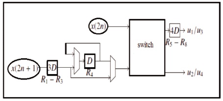
Figure 2. Reordering Shift Register (RSR) (Glittas, 2016)
The delay switch units on the left side of SW1 decouple even and odd samples. The offset is recorded between the delay switch units receiving inputs, the unit will not bare the odd input samples. These displacement log units are called RSR (Reordering Shift Register). The RSR between the store exits of the last stage of the 8-point DIF FFT and the bit reverses them. The BF2 performs two parallel butterflies operations between bit inverted data between the RSR between the last stage and the output of the 8- point FFT telegraph signal. Therefore, the top and bottom BF2 within the last stage generates the FFT outputs of the first and second data flows within the old order. The two data shapes from SW2 combine in the last stage and the thick line unit is used to represent the data shapes that it records.
The FFT pattern is divided into 6 levels (L1, L2, L3, M1, M2 and M3). The RSR is written between the L1 extensions, the proposed amount resets the register and the RSR rearranges the processed data even at the L3 and M3 levels (Glittas, 2016). The square measurements of the 8-point DIF and FFT points were performed separately on the L2 part and quantity resources. L1 and M1 information is passed to L2 and financial resources to provide SW1 in solidarity or other forms. Likewise, L2 information and financial resources can be transferred to L3 and M3 severally or contrariwise with SW2. In the above mode, the converter (SW1 or SW2) sends data at (u1, u2, u3, u4) separately to (v1, v2, v3, and v4). However, in all switch modes, the converter (SW1 or SW2) passes data from (u1, u2, u3 and u4 ) to (v3, v4, v1, and v2) individually. SW1 in N = a pair of swap mode / pair of clock cycles and in all (N / pair + 1) to previous modes N. On the other hand, SW2 is in a mode prior to all N. It is an initial hour cycle pair which is in ON (N mode) / pair of +1) to N. So SW1 and SW2 are in multiple modes at any moment and change the mode N = a few turns around the clock.
If transition data is available between (Ly to Ly + 1) or (My to My + 1, then change it switches (SW1 or SW2) to earlier mode, and if there is an information transition between Ly to (My + 1) or (My to Ly + 1), then the switch change (SW1 or SW2) to exchange mode. The signals to the SW1 and SW2 switches are provided externally and these switch management signals are changed in each (N / a couple) of clock cycles.
When transition data is available data will change the information between (Ly to Ly + 1) or (My to My + 1) to the previous position in Ly to (My + 1) or (if there is information that changes between My to Ly + 1) then if Switches (SW1 or SW2) to swap mode. The signals for the SW1 and SW2 switches are provided externally, and these switch management signals are changed in N/few hours of cycle.
The input streams to the FFT processor are X1 and X2 images. The odd and even samples of the input currents are not related to the L1 and M1 delay controllers (x1 spacing and x2 spacing). In this representation, determines the data properties and j determines the number of the set from which the FFT is calculated. The input (x(0), x(2), x(4)...) described as E(1,j).
The results of the 8 point DIF/FFT square measure were made public as E (3); (j)/O (3); (j) which feed to the third level for the calculation of FFT of 16 points. Table 1 explains the FFT operation and, together, the dissemination of information at completely different levels.
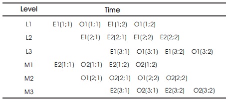
Table 1. Information Flow Through Totally Different Levels (Glittas, 2016)
Instead of using FFT radix-2 as in Figure 2, a higher FFT block can be used. In Figure 3, two 64-point radix-2 FFTs do not understand 128-point FFTs with a complex multiplier 4 factor (log (N / 2) -0.5), and the process is 8 almost the same as 16-point FFT. The complication of the N-point radix -k FFT algorithm is 4 (log (N / 2)- 0.5).
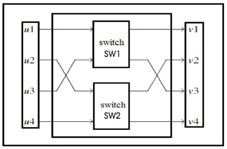
Figure 3. Internal Structure of Switch1 and Switch2 (Glittas, 2016)
Architectural design is stimulated in engineering an N / 2 information table is recorded before the first butterfly unit, and this unit is x (n) and x (n + N / 2) in parallel, using external samples separate from all samples. Within the planned design, these spreadsheet records are reused for individual inverse sample bits. Likewise, an N / 2 spreadsheet record is used before the last butterfly unit stores the prepared samples of all individual samples up to, where this registry area unit is used to partially reflect the processed samples (DIFFFT output).
A circuit that uses offset multiplexers and recorders for bit reflection plan area units. If N is an even power of r, if it matches, then the number of records needed to return N information is (-1) 2. If N is a single power of r, then the number of records needed to return N information is (√rN- 1) (√N / r-1), where r is the basis for the FFT formula. Within the proposed structure, these bit reflection circuit area units are combined into the spreadsheet record to perform a dual function.
The RSR used within the 16-point FFT and 64-point FFT architectures area unit shown in Figure 4. In fact, these structures are a gift of area unit within the locations of travel records marked with RSR. Generalized RSR for the N point shown inside Figure 4c during which c0 is N / 4 - (√N / 4-1)2 or N / 4- (√ (Nr) / 4-1) (√ N / (4r) -1). These records in c0 do RSR is used within 16-point and 64-point FFT engineering area units shown in Figure 4. In fact, this structure is a regional gift within the premium travel registration site RSR. The generalized RSR for the point N shown in Figure 4c (√ (Nr) / 4-1) (N / (4r) -1) while c0 is N / 4 (N / 4-1) 2 or N / 4 -.These records are in c0.
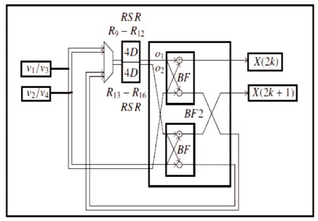
Figure 4. Structures in Level L3 and Level M3 (Glittas, 2016)
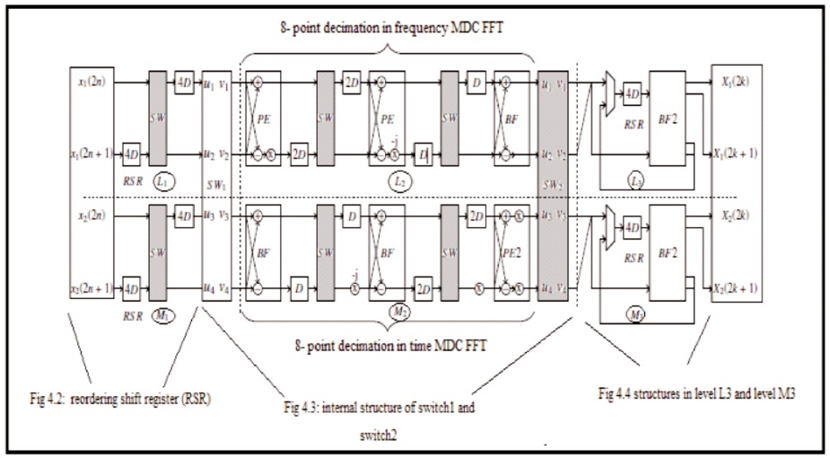
Figure 5. Implemented 16-Point Radix-2 FFT Architecture with Outputs is in the Natural Order (Glittas, 2016)
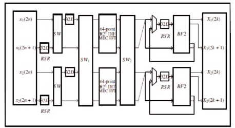
Figure 6. Proposed 128-Point Radix-23 FFT Architecture (Glittas, 2016)
Do not participate in rearranging. The RSR control signal is changed accordingly to interleave the data. If log2N is equal, then need log2N-2 multiplexer. Otherwise, need a log2N multiplier to reverse the bit.
In the proposed FFT structure, the first single N / 4 data and one N / 4 single DIF FFT region unit are converted to multiple bits when needed in parallel. Therefore, the N / 4 bit reverse algorithm is sufficient, so the required recording range for N / 4 bit reverse information is (N / 4-1) 2 or (Check (Nr) = 4-1) (N = (4r) -1 (It depends on two points).
In Figure 7, the M1 bit RSR (R1-R4) reflects the first single input file N / 4 (x (1) and (3) x (5); x (7)) and at least R5-R8 (x (1) Q (5); (3) (7)). Next, according to the knowledge of the individual inputs N / 4 (x (9); x (11); x (13); x (15)), the unit units of the inverted area of R1-R4 (x (9); x (13) )); Q (11); X (15). As shown in the second table.
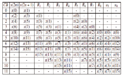
Table 2. BIT Reversal Operation in the Levels L & M 1 1 (Glittas, 2016)
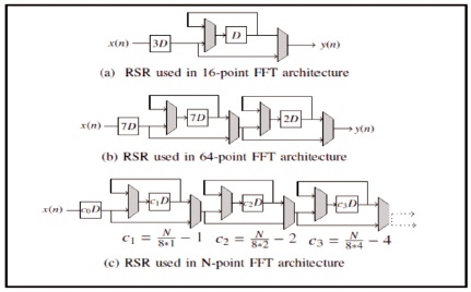
Figure 7. Reordering Shift Registers for a Different Number of Points (Glittas, 2016)
The delay correction units in L1 and M1 reverse order are individual input samples to u1, u2, u3 and u4 (SW1),
respectively. Likewise in M3, the RSR bits (R9-R12) reverse the first output data N = 4 (X (0); X (2); X (4); X (6)) and RSR (R13-R16) then N = 4 Output data (X (8); X (10); X (12); X (14 of DIT FFT shown in Table Three)). Therefore, the RSR of the L3 and M3 bits reflects the equal treated data samples v1, v2, v3 and v4 (in SW2), respectively (via o1 and o2) and feeds them to Bf2.
The radix-2 SDF DIF-FFT is implemented for 1024 point on XC5VLX50-3 FPGA Device in Xilinx ISE 14.7. The device is utilization report for 1024-point FFT is showing Figure 8. It shows that the number of flip flops, LUT is required for generation of output FFT. Also it explains that overall area is used in FPGA architecture. Also, we calculated power consumed to fetch the N=1024 operations. It is calculated that total power is 0.338W. out of that 0.07 W is used shown in the table generated by simulation .
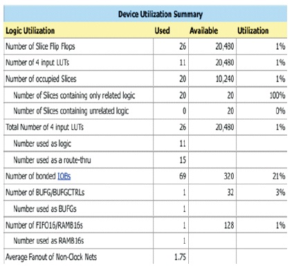
Figure 8. Device Utilization Report for 1024 point SDF DIF FFT
Later the proposed design also simulated for 1024-DIF FFT shown in Figures 13 and 14. Figure 13 gives the tabular form flip flops and LUTs, Figure 14 give the RTL logic schematic of proposed work. It gives that the power consumption and number of flip-flops, LUTs are required which is better than previous works. It shows that power consumption is almost negligible compared to leakage power.
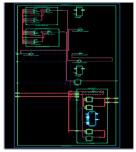
Figure 9. RTL Schematic of 1024-Point SDF DIF-FFT
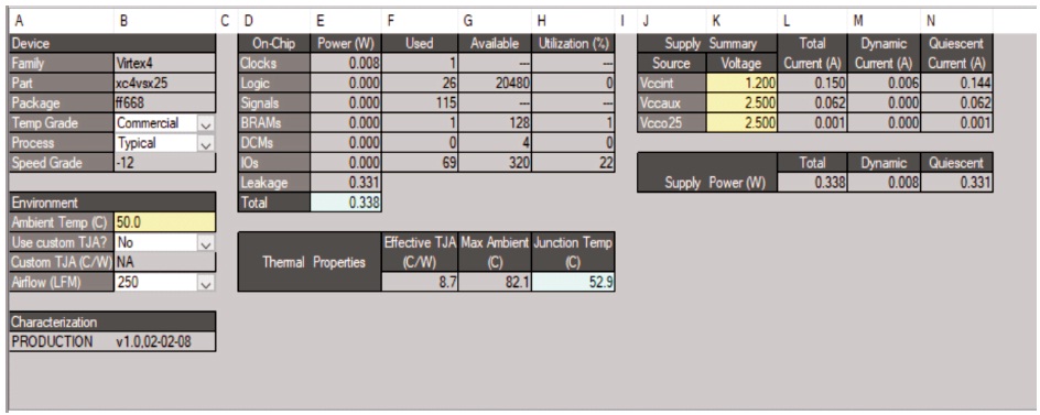
Figure 10. Power Analysis
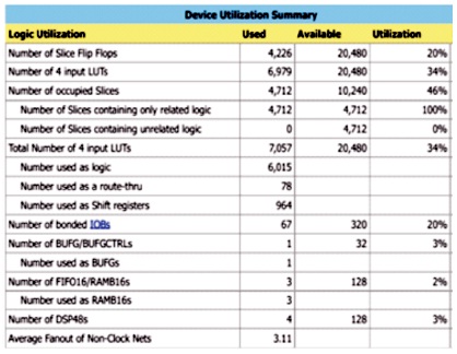
Figure 11. The Device Utilization Report for 1024-Point MDC DIF-FFT
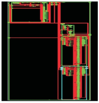
Figure 12. RTL Schematic of 1024-Point
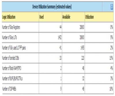
Figure 13. Device Utilization Report for 1024-Point Proposed FFT
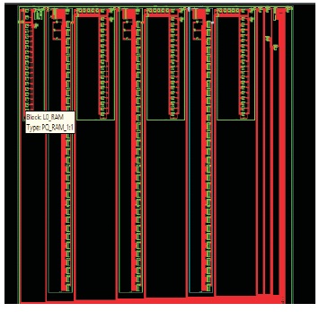
Figure 14. RTL Structures Proposed DIF-FFT
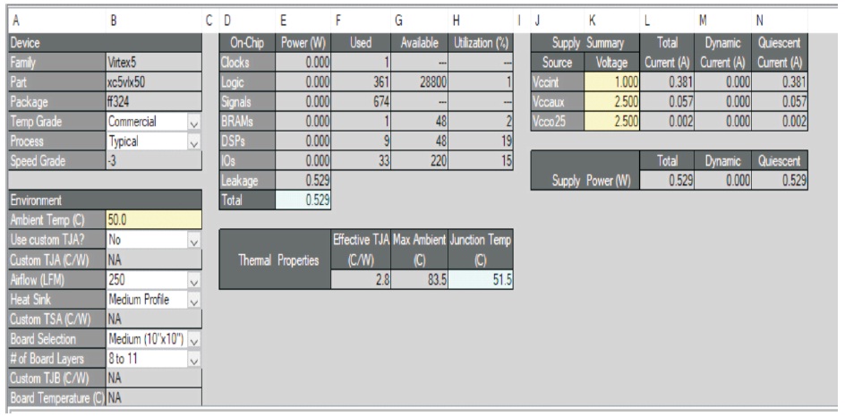
Figure 15. Power Analysis of Proposed Method
The detailed comparison is given Table 4. It shows that number of LUTs required for simulations 1452, that is three to four times less than earlier work. Simultaneously the number of FIFO is 2, it is very less than compared to other architectures. Number of DSP architecture performed with consideration of same area is 9 and this better than the other architectures. Hence, proposed 1024-FFT DIF FFT is exhibiting significant performance compare other existing methods. The proposed FFT are implementable in 5G MIMO-OFDM wireless network architectures. Leakage power consumption is one of the disadvantage of FPGA architectures, It minimize by using lower power VLSI architectures sytem design process.
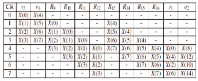
Table 3. BIT Reversal Operation in the Levels L3 & M3 (Glittas, 2016)
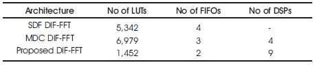
Table 4. Comparison of Device Utilization Report Implemented on XC5VLX50-3 FPGA
In this proposed method, we have proposed a novel FFT architecture for twin data stream processing. The proposed architecture is based on Radix-2 MDC architecture. The proposed architecture uses shift registers for bit reversal order operation. The same architecture does the process on two independent data streams. The proposed architecture is coded using Verilog and synthesised using Xilinx ISE 14.7. It is implemented on Xilinx FPGA device. The proposed architecture achieves less hardware complexity and achieves high throughput. This architecture is suitable for twin data processing in realtime applications like MIMO-OFDM and Wireless applications.