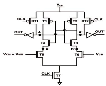
Figure 1.Current Mode Latch Sense Amplifier (Kobayashi et al.,1992)
Digital signals are crucial for transmission of information easily and securely. In digital scenario, Analog to Digital Converters (ADC) are essential for applications such as wireless communication and signal processing. Designing low power circuits that operate at low supply voltages operating at high speed plays an important role in VLSI. Among these circuits comparator is one. Comparators with high-speed, low power and reduced delay are important for faster operations in ADC. This paper presents the design of an improved Strong ARM latch comparator by reducing delay time for enhancing its speed of operation. Comparative analysis for proposed design in terms of various parameters including power, energy per conversion, delay, speed, offset and power-delay product are presented. Delay Comparison for different dynamic comparators are performed. The standard deviation of the input-referred offset for proposed design is 8.81mV at 1V supply. The proposed dynamic comparator is faster and consumes less power. At a clock frequency of 0.2 GHz and 1 mV.
In recent years, a series of developments have going on for digital dominance, and some circuits are essential to carry out a relationship between the analog and digital world in the digital domain. In trending era key professions such as medical, biochemistry shows the importance of low supply voltage, speed, and small comparator existence (Li et al., 2014). To achieve this strategy, there is a need for more comparators. Most Analog-to-Digital converters (ADC) employs comparators as their building blocks. Several high-speed ADC's like flash ADC's need high-speed, low power comparators with small chip area. The fastest comparators in CMOS technologies affected from low supply voltages, especially when looking attentively at the reality that threshold voltages of the devices have not been scaled at the same rate as the supply voltage of the CMOS processes (Goll & Zimmermann, 2009). Therefore, designing the highspeed comparators is more challenging when the supply voltage is smaller. Kobayashi et al. (1992) proposed two circuit schemes which cut the power dissipation. One was a new current-mode latch sense amplifier shown in Figure 1, which carry out the power reduction without worsen the access speed compared with the conventional current- mirror sense amplifier operation. Second one is a newtype input buffer, Static Power Saving Input Buffer (SPSIB) used for reducing static power.
Figure 1.Current Mode Latch Sense Amplifier (Kobayashi et al.,1992)
Shinkel et al. (2007) have analyzed a conventionaldouble- tail comparator, which can work at the highspeed even at smaller supply voltage. An added transistor in its design does not create any drawbacks. It has less stacking. Goll and Zimmermann (2009) demonstrated the conventional comparator. The advantages of conventional dynamic comparator is good strength against mismatch and noise. Babayan-Mashhadi and Lotfi (2013) presented a low power low voltage double-tail comparator. A conventional double tail comparator was modified for fast operation and low power consumption at very small supply voltage. Li et al. (2014) have proposed a modified StrongARM regenerative comparator by designing a pair of cross-coupled P-type transistors in the regenerative latch for reduction of reset time and to decrease the number of stacked transistors. Whenever the race condition appears in S-R latch, the cascaded S-R latch eradicates the glitches.
Razavi, (2015) investigated the StrongARM latch design. In different applications such as comparator, a sense amplifier, or a robust latch with high sensitivity can be used. It draws high transient currents from the supply and the inputs. Papadopoulou et al. (2017) proposed dual StrongARM (DSA) comparator, which functions at lowvoltage operation in deeply scaled technologies. Offset sensitivity and offset can be reduced by adding a second regenerative latch. For low-voltage applications, it is presented as a variation-tolerant low-offset comparator.
Wang et al. (2019) presented a new dynamic comparator with a novel trans-conductance enhanced latching stage, which is suitable for low power high-speed operation. In their proposed design, the cross-coupled transistors in latch structure are biased in strong inversion region over the reset phase, which enhances the total effective trans-conductance of the latch at the starting of the comparison phase and decreases the delay and energy consumption. Kim et al. (2017) have proposed an enhanced asynchronous CSDA based comparator capable of achieving a superior latency versus quiescent power dissipation in the near-threshold regime. The twostage comparator is capable of attaining the better energy consumption per sample versus throughput than the CSDA comparator, but the differences become smaller at the near-threshold voltage regime. It performs in terms of robustness against process mismatch and power supply variation.
Xu and Abidi (2019) developed a simple, physicallybased analysis for the internal workings of a regenerative comparator. It brings us to the key role of the dynamic preamplifier that is present in most comparators. They compare the widely used StrongARM comparator with the evolved version of the double tail topology for the irrelative merits of noise, speed, and operation at low supply voltages.
Bindra et al. (2018) implemented a latch-type comparator with a dynamic bias pre-amplifier. The proposed comparator offers a low overhead solution to reduce the energy consumption of the pre-amplifier. Hussain et al. (2017) proposed a modified dynamic comparator, which is fast and consumes less power. The comparator consists of a low gain amplifier connected to latch circuit. During the evaluation period, the inputs are amplified and the outputs are latched during the regeneration time. Yazid, (2018) proposed a new method for reducing the input-referred thermal noise of dynamic comparator circuit without increasing the load capacitance. This circuit can be set to operate in both low-noise mode and standard mode using a single digital control signal.
Comparator is an electronic device, that consist of two input terminals and one output terminal, which compares two voltage or current and outputs a digital signal indicating the larger signal. Comparators can observe the magnitude or shortfall of the signal from maximum or minimum extent.
The main objective of the work is to design a dynamic comparator works at high sampling frequency with less delay time. The new proposed topology is analyzed and then tested.
StrongARM latch comparator is a well-known topology. Some features are do not consume static power, producing rail for rail output, High input impedance, small input referred offset and good robustness against noise and mismatch(Carusone et al.,2012; Wicht et al., 2004)
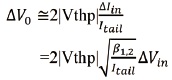
The authentic StrongARM latch was first proposed by Kobayashi et al. (1992) and Razavi, (2015). To enhance the robustness re-fashioning for Figure 2a has been done which shown in Figure 2b. The StrongARM latch comparator consists of 11 transistors (S1, S2, S3, and S4), cross-coupled transistors (M5,M6,M3,M4), input transistors (M1 and M2) and one tail current transistor (Mtail). Operation of StrongARM latch comparator is shown in Figure 3 and the operation phases of the comparator as follows: During reset phase the CLK goes low, Mtail becomes OFF and the internal capacitors at the nodes A, A', p and q charges to VDD through the switches. When the CLK is high, amplification phase begins turning all switches OFF and granting the capacitors to discharge through Mtail. M1 and M2 are biased by a constant tail common mode voltage (VCM). Hence, these transistors are always ON. When a small differential voltage (Vdiff) is present between the gates of M1 and M2, it causes a slight difference in current through these two transistors. Consequently, the capacitors at the nodes p and q are discharged at slightly different speeds, therefore, the voltages at these nodes drop at different rates. M3 and M4 turns ON when the voltages at nodes p and q reaches threshold voltage (Vthn). After that, the voltages at nodes A and A' begin to drop at different rates. Regeneration phase starts when the voltage at either A or A' drops to the difference of VDD and Vthn, turning either M5 or M6 ON, and the other transistor remains OFF due to the crosscoupled configuration. As an outcome, the last voltages reach VDD at either node (A or A') and zero volts for the other node, depending on the polarity of Vdiff. The outputs are taken from nodes A and A' are fed to the inverters.
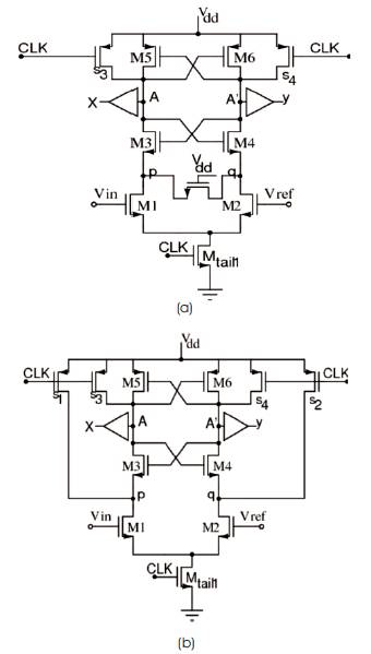
Figure 2. (a) Modified Current Mode Latch Sense Amplifier (Razavi, 2015) (b) Schematicof StrongARM Latch Comparator (Razavi, 2015)
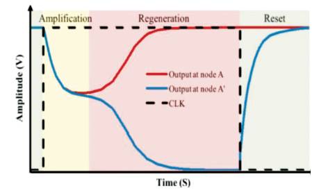
Figure 3. Operating Phases of StrongARM Latch Comparator
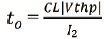
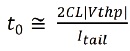
Delay in comparator is due to two parameters first term is the discharge delay (to) and the second term is the latching delay (tlatch) of two cross-coupled inverters.

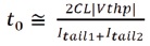
The discharge delay is given by
Since,
The output voltage oscillation  boosted from internal voltage difference ΔV0 at output voltage drop (A, A'). The half of voltage resource is considered as the threshold inverter latch (Babayan-Mashhadi & Lotfi, 2013; Ziaei, 2016).
The latching delay is given by(Choi & Tsui, 2012)
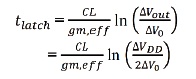
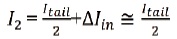
tlatch is depends on the ΔVout & ΔV0 via logarithmic relationship. The voltage difference ΔV0 at nodes A and A' at t = t0 is obtained as,
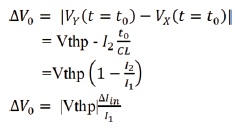
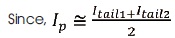
Since,| I2 - I1| =ΔIin, here I1 can be assumed as half of Itail.
β1,2 is the conductivity coefficient of M1 and M2 transistors. Substituting the above derived equations, latching time delay is given by,
From relation (7), the delay time depends on some factors. The delay time has a direct relation with load capacitor CL, which reduces with increasing tail FET current. For delay time reduction, it is better to increase Itail (Schinkel et al., 2007).
In common, to enhance the performance of the circuit, it is desired to increase the current. This is achieved by adding a tail FET to the conventional design.
The proposed design of StrongARM latch comparator is shown in Figure 4a, which consists of 12 transistors. The purpose of adding a FET as a tail is to increase the current which results in decreasing the amplification delay. And in latching period, it works same as conventional comparator. By this power consumption, delay time can be reduced. Transient response of proposed design is shown in Figure 4b.
Figure 4 a) Proposed Design of StrongARM Latch Comparator (b) Transient Response of Proposed Design for VCM = 500mV, Vin =1mV, Vdd = 1V

The discharge delay is given by,
The output voltage oscillation boosted from internal voltage difference ΔV0 at output voltage drop (u, v). The half of voltage resource is considered as the threshold inverter latch (Babayan-Mashhadi & Lotfi, 2013; Ziaei, 2016).
The latching delay is given by (Choi & Tsui, 2012)
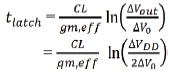
tlatch is dependent on the ΔVout & ΔV0 via logarithmic relationship. The voltage difference ΔV0 at nodes u and v at t = t0 is obtained as,
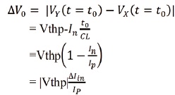
Since,| Ip – In | =ΔIins
here Ip can be assumed as half of Itail1
Substituting the above derived equations, latching time delay is given by,
Double tail comparator has less stacking, therefore it can be operated at lower supply voltages than Strong ARM latch comparator. Schematic of conventional double tail comparator is shown in Figure 5
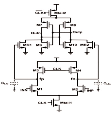
Figure 5. Schematic of Conventional Double Tail Comparator (Babayan-Mashhadi & Lotfi, 2013)
In order to compare the proposed comparator with the conventional and different dynamic comparators, all the circuits are simulated in a 90nm CMOS technology with VDD=1V. Analysis of the parameters like delay, power, power delay product, energy per conversion has been done. From the simulation results, proposed comparator is faster and dissipating lesser power.
From the delay time versus supply voltage graphs shown in Figure 6(a-d), as supply voltage increases delay time decreases in StrongARM latch comparators and proposed comparator. The proposed design has less delay when compared to Strong ARM latch comparator. At VDD = 1 V, VCM = 500 mV, for ΔVin =10 mV, the delay for in proposed is 60ps and for conventional delay time is 126ps. Different dynamic comparators were simulated in 90nm CMOS Technology and their delay times were calculated. In Figure 6(d), comparative graph is drawn based on delay versus differential voltage. From these, as differential voltage increases, the delay time decreases.
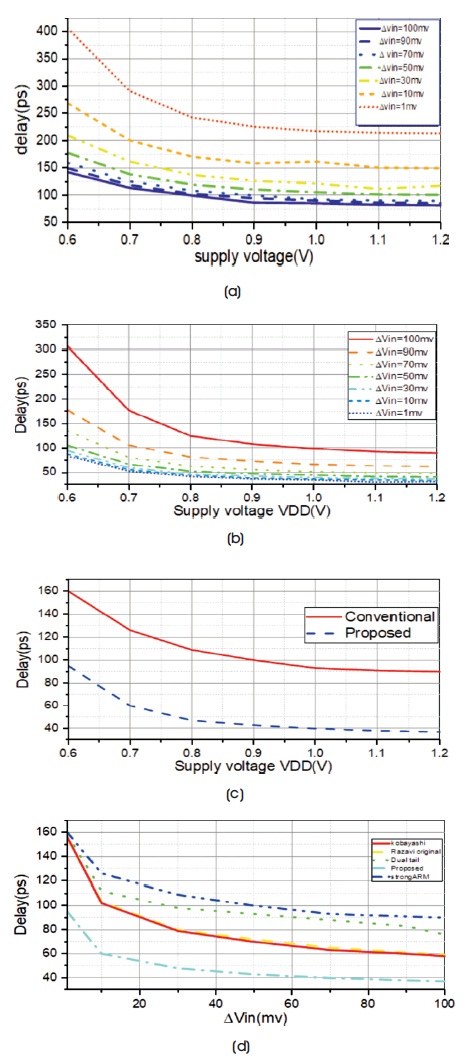
Figure 6.(a) Delay Time Versus Supply Voltage for Strong ARM Latch Comparator at VCM=500 mV, (b) Delay Time versus Supply Voltage for Proposed Comparator at VCM=500 mV, (c) Delay Time versus Supply Voltage Comparison for Proposed and Conventional Comparator at VCM=500 mV, (d) Delay Time versus Supply Voltage Comparison for all Simulated Comparator at VCM=500 mV
In fabricating the transistors, variations in threshold voltage can cause oxide thickness, which leads to input-reffered offset in the circuit and restrict the minimum Vdiff.
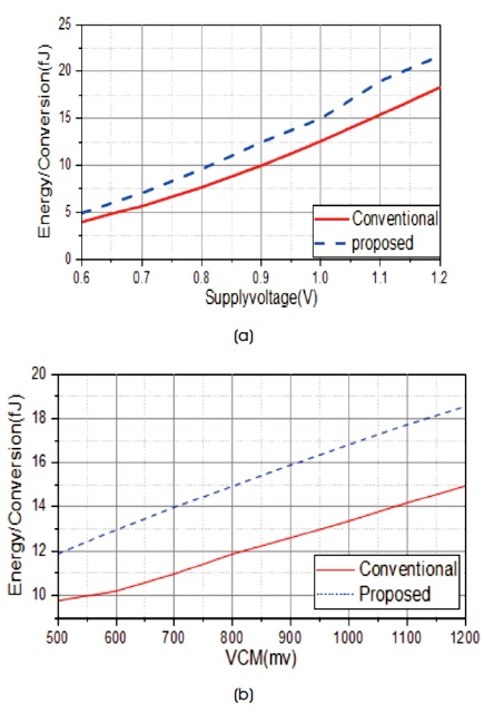
Figure 7. (a) Energy per Conversion versus Supply Voltage Comparison for Proposed and Conventional Comparator at VCM=500 mV, (b) Energy per Conversion versus VCM Comparison for Proposed and Conventional Comparator at VDD=1V
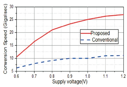
Figure 8. Speed Conversion Versus Supply Voltage Comparison for Proposed and Conventional Comparator at VDD=1V.
The critical MOSFETs in both conventional and proposed designs are M1, M2. To resemble this variation, Monte Carlo analysis has been done. Figures 9 (a, b) shows a histogram plot, which results in a standard deviation of 8.81mV for proposed design compared to standard deviation of 10.261mV for conventional design, respectively.
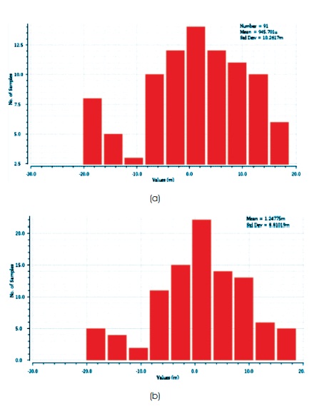
Figure 9. (a) Monte Carlo Offset Analysis for Conventional Design, (b) Monte-Carlo Offset Analysis for Proposed Design
Performance comparison for different dynamic comparators is shown in Table 1. In generic, the proposed design offers faster performance with more confined standard deviation as shown in Table 2.
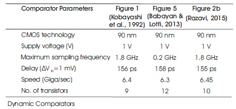
Table 1. Performance Comparison for Different
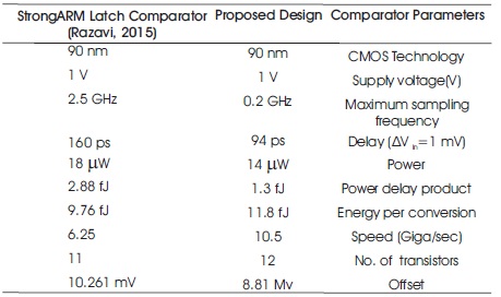
Table 2. Performance Comparison of StrongARM Latch Comparator and Proposed Design
In this paper, an improved StrongARM latch comparator is presented. In the proposed design, by placing another tail FET, the current is increased which decreases the amplification delay and increases the transconductance of transistors, leading to a total offset reduction. Cadence Virtuoso simulations and evaluations of our design in 90 nm CMOS technology, shows that our proposed design works at high sampling frequency with less delay and at high-speed.