(1)
In recent trends, the industry and most researchers are focusing on the scale down of CMOS technologies to improve the speed and leakage power reduction in the circuits. These unsought leakage currents should be minimized for smooth functioning of the circuits. To develop such type of leakage-free CMOS circuits could be challenging. The main objective of the project is to address the issues over leakage power reductions, delay and efficiency. We present a circuit technique for mitigating MOSFET through controlling the voltage at source terminal of the MOSFET. In this paper we will present CMOS INVERTER, NAND, NOR, XOR using Lector technique. The simulation results are obtained with the aid of MENTOR GRAPHICS of 120 nm technology and also the comparisons of power dissipation by using with and without Lector techniques and with other techniques.
As the impact of electronic systems on every walk of life is becoming more and more, the demand for very low cost, very small and very reliable systems is also increasing exponentially. The rapid development of the semiconductor technology leads to very small systems with the power of super-computers of the last decade. The design of such small systems is now witnessed in all fields like mobile communications, industrial electronics and omnipresent computing. Electronic circuits are characterized by reliability, low power dissipation, extremely low weight and volume and cost efficiency with a high degree of computation and complexity. The technology advances have largely contributed to miniature transistor size, reduction power consumption and reliable service enhancement as a major factor. VLSI Technology has been the enabler to advance the current age of electronics and communications. Nearly 90% of the world manufactured electronic circuits are made of silicon using CMOS Technology (Ghosh et al., 2013; Nandyala & Mahapatra, 2016; Verma et al., 2016).
In the following sections, we will discuss different techniques to reduce leakage power in the VLSI circuit. low-power design is one of the most critical issues facing nanometer Very Large Scale Integration (VLSI) circuit design. With the continuous scaling of the technology, the power consumption has become a bottleneck for widely used high-speed, battery powered portable devices. CMOS technology is used relatively because of its highper formance and cost-effectiveness (Prasad & Shyamala, 2014; Yeo & Roy, 2009). VLSI circuits are used because of its low power and less area requirement (Zhigang et al., 2017). CMOS technology scaling has improved speed but the leakage current remain as an adverse effect. For the smooth operation of the circuits, these unsolicited leakage currents should be reduced (Ray et al., 2016). LECTOR Technique is a technique for reducing the consumption of leakage power in CMOS circuits without affecting the dynamic power of the circuit (ASICSOC, n.d.; Dilip et al., 2012; Gangele & Patra, 2015; Goankar, 2015; n.d. Saxena & Soni, 2013; Yousif et al., 2016). In this paper, the performance of Full Adder, XOR and XNOR implemented with NAND gates using LECTOR technique is compared with the basic model and power dissipation and delay are compared.
the following sections, we will discuss different techniques to reduce leakage power in the VLSI circuit. There are mainly two types of power dissipation in the CMOS Circuit. They are dynamic power dissipation and static power dissipation or leakage power. The dynamic power dissipation mainly causes due to the switching of the transistors in the CMOS circuit (Yang et al., 2004). It is given by Equation (1).
Here “α” is the switching activity i.e. the clock cycles in which the circuit switches, Cload is the load capacitance, Vdd is the supply voltage and “f” is the clock frequency. The second type of power dissipation i.e. static power or leakage power generally occurs when the circuit is not switching or in standby mode. As the technology is scaling, this has become significant now a days. The major component of static power are, a) Reverse biased pn-junction leakage current, b) Sub threshold leakage, c) GIDL and GIBL leakage currents, d) Gate oxide Tunnelling current.
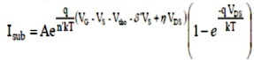
The junction leakage is caused due to minority carrier diffusion and drift near the edge of depletion regions and also from generation of electron holes pairs in the depletion region of reverse bias junctions. The reverse biased pn-junction current is given,

Is depends on the doping level, area and perimeter of diffusion region.
Subthreshold leakage current is the weak inversion conduction current between source and drain in an MOS transistors, occurs when gate voltage is lower than threshold voltage. The subthreshold leakage current increases with respect to the temperature and it also increases as threshold voltage scaled down along with the power supply voltage for better performance (Chowdhury et al., 2012).
The various parameters that affects the subthreshold leakage current are, drain induced barrier lowering, body effect, narrow width effect, effect of the channel length and effect of the temperature.
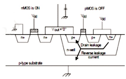
Figure 1. Reverse Biased pn Junction Leakage
The gate induced drain leakage (GIDL) is due to the high electric field, induced by the gate potential, in the gate drain overlap region. The Drain Induced Barrier Lowering (DIBL) occurs when the drain potential increases. The pnjunction between the drain and the substrate becomes more reverse biased, so the depletion layer grows and reduces the volume controlled by the gate. As a result VTH decreases as VDS increases.
When there exist a high electric field across a thin gate oxide layer, gate oxide tunneling electron can result in leakage. Electron may tunnel into the conduction band of the oxide layer, this is called Fowler-Nordheim tunneling. There can also be direct tunneling through the silicon oxide layer.
We have seen the leakage power dominating the total power consumption, so it is necessary to reduce the leakage power.
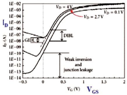
Figure 2. Response of GIDL and DIBL
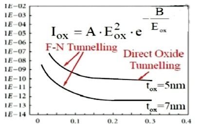
Figure 3. Gate Oxide Tunnelling Leakage,1ox /E2vs 1/E
We have seen the leakage power dominating the total power consumption, so it is necessary to reduce the leakage power.
The fundamental building blocks of digital systems are logic gates. They are circuits in which the output depends upon the inputs according to the logic rules. The electronic circuits that operate on one or more input signals to produce an output signal are known as logic gates.
The NAND gate is called a Universal gate because it can perform all the three basic functions of AND, OR, NOT gates. The NAND gate is a AND gate followed by NOT gate. It is a NOT- AND operation. It may have two or more inputs but only one output. The logical symbol of NAND gate is given in Figure 4.
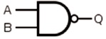
Figure 4. Logical Representation of NAND Gate
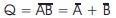
It is clear from the truth table of two input in NAND gate that the output is 1 when either A or B or when both the inputs are at logic '0'. For all input value combinations AND gate output is exactly opposite to the output of NAND gate. The logical expression for the output is given by,
The NAND gate can perform the OR function by inverting the inputs. The OR gate with inverted inputs is called bubbled OR gate or negative OR gate. The NAND gate is also called active low OR gate.
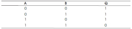
Table 1. Truth Table of a NAND Gate
Figure 5. Logical Representation of XOR Gate
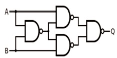
Figure 6. Realization of XOR Gate using NAND Gate
A basic XOR gate is a two-input single output logic gate, whose output is assumed to be HIGH only when one of its inputs are HIGH. XOR can simply be defined as one or the other but not both.
If input variables are represented by A and B then the logical expression for output is given by,

The most important application of XOR gate is in parity generation and detection. It is also known as staircase switch. XOR gate acts as an inverter for control input of logic '1'.
The circuit which consists of an interconnection of logic gates whose outputs at any instant of time are determined from a present combination of inputs only is defined as a combinational logic circuit. The 'n' input binary variables come from external sources; the combinational logic circuit produces 'm' output variables by the internal logic connections and go to an external destination. Every input and output variables are contacted physically as an analog signal whose values are interpreted to be a binary signal that represents logic HIGH and logic LOW (Maheswari, n.d.).
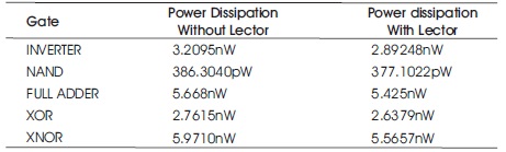
Table 2. The Truth Table of XOR Gate
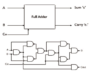
Figure 7. Full Adder Realization using NAND Gate
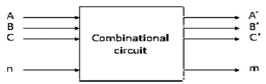
Figure 8. Representation of Combinational Circuit
For 'n' input variables, there are 2 possible combinations of binary inputs.
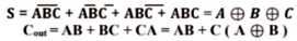
The Full Adder is known as a combinational circuit performing the arithmetic sum of three input bits. It consists of three input variables that are identified by augend, addend and the carry bit. The SUM and CARRY are produced by the two output variables.
From the truth table given below, the logical expressions for Sum (S) and Carry (Cout) are,
In the design of CMOS VLSI circuits, power dissipation is one of the major considerations. The minimization of the threshold voltage due to voltage climb up leads to increase in subthreshold leakage current and static power dissipation in CMOS circuits, CMOS gates are designed using leakage Control (LECTOR) Technique which results in the reduction of the leakage current without any impact on dynamic power dissipation. In any supply to ground path, a state with more than one transistor OFF in a path from the source voltage to earth is far less leaky than a state with only one transistor OFF. In each CMOS logic gate, two leakage control transistors are introduced such that one of the LCT's is close to its cut-off operating region.
The LCT1 and LCT2 leakage control transistors are inserted between the nodes N1 and N2 and they act stacked like transistors that are self-controlled.
In this paper, we implement LECTOR Technique with NAND gate. A CMOS NAND gate with the addition of two leakage control transistors is shown in the Figure 9. Two leakage control transistors LCT1 (PMOS) and LCT2 (NMOS) are introduced between the nodes N1 and N2 of the pull-up and pull-down logic of the NAND gate. The drain terminals of the transistors LCT1 and LCT2 are wired together to form the output node of the NAND gate. The source terminals of the transistors are wired to nodes N1 and N2 of pull-up and pull-down logic respectively. The switching of the transistors LCT1 and LCT2 are controlled by the voltage potentials at nodes N2 and N1 respectively. This setup guarantees that one of the LCT's is always near its cut-off region regardless of the input vector applied to the NAND gate. lector does not require any other additional control circuitry to monitor the states of the circuit. Self-biased transistors have their gate and their drain terminals wired together as a single node. Thus no external control circuitry is required.
Table 3. Truth Table for Full Adder
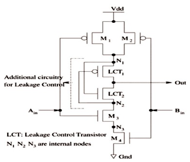
Figure 9. Two Input LCT NAND Gate
In this paper we are implanting basic gates like inverter, NAND, XOR, XNOR gates and combinational logic circuits like full adder using proposed techniques. Here we are comparing present lector techniques with other techniques. Observing the simulation results the proposed technology consume less power.
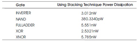
Table 4. Power Dissipation using Lector Technique
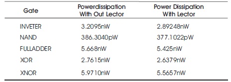
Table 5. Power Dissipation using Other Techniques
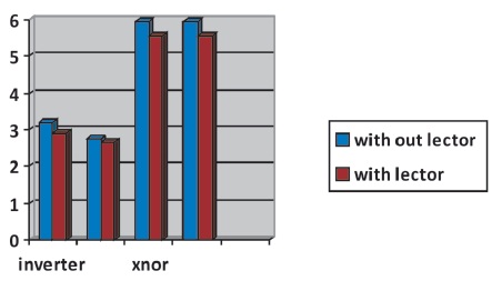
Figure 10. Graphs for Power Comparison
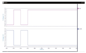
Figure 11. INVERTER Circuit Waveforms
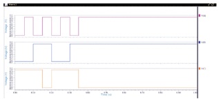
Figure 12. NAND Circuit Waveforms
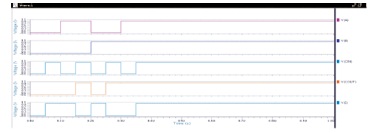
Figure 13. Full Adder Circuit Waveforms
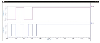
Figure 14. XOR Circuit Waveforms
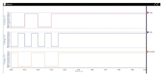
Figure 15. XNOR Circuit Waveforms
Power dissipation and delay are the major parameters that affect the performance of the circuit. The performance of a simulated basic full adder, XOR, XNOR model and the LCT full adder, XOR, XNOR simulated model is compared. The full adder, XOR, XNOR with LCTs offer a reduction in leakage power as the LCT is in near cut-off region always. However, the increase in a number of logic levels increases the delay as the delay is considered by taking the average of delays at the gates of each logic level. The suggested method overcomes the constraints of current leakage reduction techniques with an average reduction in leakage of 82.5%. When the speed of operation is needed, the reduction in a number of logic levels will improve the performance of the circuit decreasing the delays.