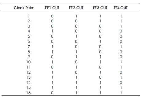
Table 1. Pattern Generation by LFSR
Linear Feedback Shift Registers (LFSRs) are basic building block of Built in Self-Test (BIST) circuits. Tri State Skip (TSS) method of pattern generation using LFSR is used in this research to form TSS LFSR and the results obtained for it are compared with other LFSRs, viz: pipelined LFSR, Gray LFSR, Binary Counter, and Gray Counter. The key objective of this paper is to calculate the area and power consumption of TSS LFSR. The results show that the power consumed by TSS LFSR is comparatively less than other LFSRS studied in comparison. Moreover, the number of gates used when using Transmission gates to design TSS LFSR is quite less than other LFSRs, thereby, minimizing area requirement.
Minimizing power dissipation in VLSI circuits increases battery lifetime and reliability of the circuit. In general, the power dissipation of Complementary Metal Oxide Semiconductor (CMOS) circuits can be divided into two main categories: they are static power and dynamic power ( Tenentes et al., 2010; Voyiatzis, 2008). The power consumed in the test mode can be more than twice the power consumed in normal mode. The correlation between the successive functional input vectors during normal operation is considered to be high compared to the correlation of test vectors in the test mode. However, for test vectors generated by a Test Pattern Generator (TPG), such as LFSR, there is no definite correlation; this will increase the switching activity of the circuit ( Gunavathi et al., 2006).
A LFSR is represented to as a polynomial, which is known as characteristic polynomial used to determine the feedback taps, which determine the length of the random pattern generation. The output of LFSR is a combination of 1's and 0's. For example, if the taps are in the 3rd, 4th bits, the resulting LFSR polynomial is X4 +X3 +1, Where, '1' is the polynomial does not correspond to a tap. The powers of the terms represent the tapped bits, counting from the left. If (and only if) this polynomial is primitive, then the LFSR is maximal. The LFSR can be maximal only if the number of taps is even. The tap values in a maximal LFSR will be relatively prime (Nourani et al., 2008). There may be more than one maximal tap sequence for a given LFSR length. Its output for various condition of input is expressed in Table 1.
Table 1. Pattern Generation by LFSR
Linear Feedback Shift Register (LFSR) is a shift register, whose input bit is a linear function unlike most everyday devices, whose inputs and operations are effectively pre-defined ( Corno et al., 1998). There are many methods for generating very efficient sequences through LFSR. LFSR when clocked moves the signal through the register from one flip flop to next. Some of the outputs are combined in exclusive-OR configuration to form a feedback mechanism.
Figure 1 shows the general architecture of the proposed TSS scheme and it shows the functional or logical blocks of the proposed algorithm with memory and Circuit Under Test (CUT). The proposed structure has four main components, namely D-flip flop, Spilt test data set, Match test set and compressed bit selecting/skipping set. First the whole test vectors are stored in memory, which feeds to D-flip flop counter each time of testing. These test sequences are randomly generated. Then the present test sequence is compared with the next consecutive test sequence using filling algorithm. It generates a different state value based on the correlations among the different test sequences. Finally, those test sequences are sent to CUT ( Whetsel, 2000; Goud & Madhavi, 2015). Figure 2 shows low power LFSR after applying TSS algorithm.
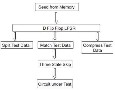
Figure 1. General Architecture of TSS Scheme
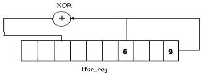
Figure 2. Low Power LFSR After Applying TSS Algorithm
Table 2 shows the power comparison between TSS LFSR which is Low power LFSR and normal LFSR, Pipelined LFSR, Gray LFSR, and Binary up LFSR. Area comparison of various LFSRs with respect to gate count is shown in Figure 3. Table 3 and Table 4 shows the comparison between the existing algorithms (TFSS) and proposed TSS algorithm for peak and average power analysis for ISCAS benchmarks in testing.
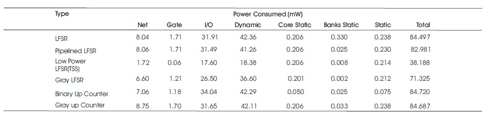
Table 2. Power Consumed by Various LFSRs
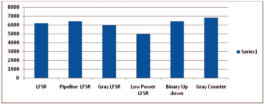
Figure 3. Area Comparison by Various LFSRs with Respect to Gate Count
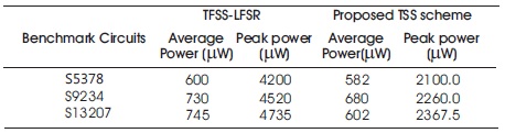
Table 3. Average and Peak Power Consumed by TFSS and TSS
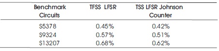
Table 4. Area Overhead by TFSS and TSS
The technique described here is the stuck-at fault model, which is the widely used fault model. However, delay testing based on a delay fault model, is becoming increasingly important on the test flow. Delay testing is used to verify if a circuits meets its timing specification. Although several low power approaches have been proposed for stuck-at fault model tests, few techniques of low power delay testing have been proposed despite its importance in today's systems. Thus, techniques and methodologies for addressing this problem can be suggested ( Nourani et al., 2008).
Recent developments in semiconductor design techniques make it possible to integrate millions of transistors in a single chip to form System-on-Chip (SoC). However, problems related to SoC test still exist. These problems include test time, test storage, and test power ( Stroele & Mayer, 1997). The test time problem and test power problem are highly related to each other. In SoC testing, each core is independently tested and the interconnected wires between the cores are tested. If several cores are tested serially, this will reduce the average power consumption, but will increase the test time. If all or some of the cores are tested concurrently, this will decrease the test time but will increase the power consumption.
Therefore, the average power consumption restricts the number of cores that can be tested concurrently. Thus, if power consumption in SoC can be reduced, a larger number of cores can be tested concurrently, thereby reducing test time.
While this paper explores some properties of the LFSR and has developed some techniques for low power testing and high fault coverage. There are several points that can be investigated further in order to develop other techniques that are an improvement on existing techniques. In this section, a number of future research directions in the field of testing will be briefly described.
Since many of the techniques presented in this paper are based on new properties and observation about the behavior of LFSRs, search can help in developing new techniques that improves the fault coverage, power consumption and any other parameters related to test. Furthermore, since the LFSRs have many other applications other than testing of digital VLSI circuits, many properties can be useful in these applications, such as cryptography (Hatami et al., 2005).
Despite the fact that there are many proposed techniques to minimize power consumption during test, there appears to be only a few solutions dedicated to memories. During normal system operation, only one memory bank can be accessed at any given time from the several banks included in the memory. By contrast, it is desired to test all banks concurrently in order to reduce the test time during test and to simplify the BIST control circuit. Unfortunately, this can lead to very high power consumption compared to normal operation ( Tenentes et al., 2010). Thus reducing test power in memories is one of the hot directions for future research.