Table 1. The EOS / ESD Failure Percentage as Total Failure Modes Studied by the different Authors over the Years (Huang et al., 2001)
This paper discusses the trends in ESD protection design used in I/O libraries in advanced CMOS and FinFet technologies. The trends and guidelines are provided predominantly for low voltage I/O libraries that are commonly used for general purpose interfaces and industrial low voltage interfaces such as, GPIO, DDR, LVDS, etc. Additionally, the impact of technology scaling on ESD qualification targets for CDM stress is considered.
Electrostatic Discharge (ESD) is a common phenomenon in the nature. Its name comes from the fact that different materials can carry static positive or negative charges resulting into a built-in static voltage. The amount of this static charge depends on the material characteristics and from external parameters like the relative humidity. But once the statically charged material is put in contact with a grounded object (large enough to act as ground), charge balance will be restored through a discharge of the charged material towards the ground. The discharge is extremely fast, in the order of tens of nanoseconds. ESD is a subset of the class of failure causes known as Electrical Overstress (EOS).
As microelectronics technology continues to shrink in nano metric dimensions, ESD damage in integrated circuits has become one of the major reliability issues. The thinner gate oxide and shallower junction depth used in the advanced technologies make Integrated Circuits (ICs) very vulnerable to ESD damage. Several studies carried out over the past two decades ranked ESD and EOS (electrical overstress) as the major cause for field returned ICs, as it is shown in Table 1.
Table 1. The EOS / ESD Failure Percentage as Total Failure Modes Studied by the different Authors over the Years (Huang et al., 2001)
As CMOS Field-Effect Transistors (FETs) shrink from 32 nm to 22 nm or beyond, the need for Short Channel Effect (SCE) control and the increase of driving current have forced CMOS device technologies to move from “planar” to “FinFET” device architecture (Okano et al., 2005). ESD is considered as one of the major reliability roadblocks of the FinFet technologies, since FinFet devices show heavy degradation of ESD performance, which is attributed to the significant loss of silicon volume and the failure occurs as a consequence of selfheating in one form or other.
In this paper, the trends in ESD protection design in I/O libraries are analyzed for 40 nm, 28 nm bulk CMOS, and 16 nm FinFet technology nodes. Also, the ESD qualification targets for I/O libraries implemented in 16 nm FinFet technology are discussed.
The proposed ESD scheme was developed to provide the optimal ESD solution for the pad limited multicore chips for multimedia applications. The main ESD protection network is a dual diode and active triggered power rail clamp implemented in the distributed manner, which is typical for FSL I/O libraries (Stockinger et al., 2005; Semenov & Somov, 2008). This distributed ESD protection network is suitable for both FlipChip (FC) and Wirebond (WB) packages. 40 nm CMOS process has 7 metals stack and provides 2.5 V dgo50 transistors with RPO (Resistor Protection Oxide) layer for I/O and ESD design. The ESD protection targets are 2000 V HBM, 200 V MM, 500 V CDM. The ESD protection network has the following components:
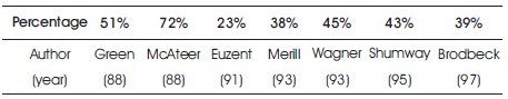
The block diagram of ESD protection network developed for digital 1.8 V / 2.5 V / 3.3 V GPIO or DDR cells and concept of ESD trigger circuit are shown in Figures 1 and 2, respectively.
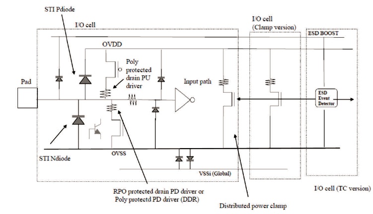
Figure 1. Block Diagram of Digital I/O ESD Protection

Figure 2. Concept of ESD Trigger Circuit
A specialized I/O & ESD library has been designed to handle I/Os that require switchable 2.5 V/1.8 V functionality. Since only 1.8 V DGO (Dual Gate Oxide) transistors suitable for the design of IO drivers were available in 28 nm CMOS process, the ESD clamps and output drivers were designed based on the cascoded (stacked) transistors.
Similar to the ESD protection strategy previously implemented in 40 nm CMOS process, the ESD protection in I/O banks in 28 nm CMOS process is achieved by a distributed active NMOSFET rail clamp network between the VDD_IO and VSS busses in this bank. This rail clamp network provides a robust and low-resistive current shunt path between VDD_IO and VSS during an ESD event. The rail clamp network is controlled by a transient Trigger Circuit (TC) which detects ESD events and activates the rail clamps when necessary. These trigger circuits are placed in ESD I/O trigger cells and ESD termination cells. However, one TC can only drive a limited amount of NMOS rail clamp. This limitation arises from the total capacitive load of the rail clamp gates that need to be quickly charged by the TC output stage during ESD. Consequently, ESD I/O trigger spacer cells have to be placed in a defined frequency, depending on the implemented ESD protection strategy. At least one trigger containing cell is required for any four functional GPIO cells with ESD clamp in any I/O bank.
During an ESD event, multiple rail clamp devices and TCs are designed to work simultaneously. However, due to the resistive nature of power busses and the associated voltage drops across these busses, only a limited number of rail clamp devices, i.e. the ones in close proximity to the zapped and grounded pads, participate in the current shunting. To route ESD signals to all the Trigger Circuits (TCs) and rail clamp devices within a supply bank, the esd_boost and esd_trigger busses are needed. Therefore, they must be continuous throughout the I/O bank as well. The usage of esd_boost and esd_trigger busses in ESD protection network is illustrated in Figure 3 that shows the block diagram of analog cell that was designed for 28 nm 2.5 V / 1.8 V GPIO library. The analog cell schematic consists of an enhanced diode and stacked clamp network terminated by a resistor bank with 4 pin connections (PAD_R1, PAD_R2, PAD_R3, PAD_R4). Internal circuits must be connected to the analog cell through one or more of these resistors.
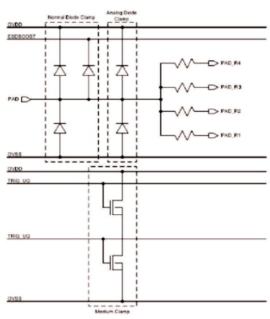
Figure 3. Concept of Analog Cell with ESD Protection
Protection of individual I/O pads is achieved by large ESD diodes from the VSS bus to the I/O pad and from the I/O pad to the VDD_IO bus. The ESD diodes dissipate the ESD current from the I/O pad to either one of the power busses, depending on the polarity of the ESD event. Any space between adjacent I/O pads must only be filled with filler cells provided in the I/O library. The block diagram of developed ESD protection network is shown in Figure 4.
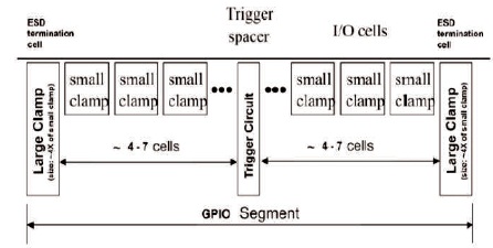
Figure 4. Block Diagram of ESD Protection Network Implemented in 28 nm GPIO Library
The ESD protection network was designed to meet 2 kV HBM and 500 V CDM (12 A peak current) ESD requirements on all external pins. The ESD network was not designed to any definite Machine Model standard, as MM is considered obsolete by the industry.
The 16 nm FinFet design challenges represent an evolutionary enhancement of problems already seen at advanced CMOS process nodes. But the 3D nature of FinFET transistors adds some new challenges summarized below:
Migration of ESD devices from planar to 3D has been a challenge largely because of reduced junction area, self heating effects, higher fin related sidewall/ junction defects, and increased parasitic resistance and capacitance (Singh et al., 2014; Li et al., 2014; Lee et al., 2015; Chen et al., 2016).
16 nm FinFet GPIO libraries were developed for Flip-Chip (FC) and Wire- Bond (WB) packages with 11-metal (11M) and 9-metal (9 M) process options. In this paper, the ESD protection network optimized for Flip-Chip 11M 1.8 V GPIO library is considered (Meng et al., 2017). The physical architecture of I/O library includes three regions: IO, ESD edge, and De-Cap edge, as shown in Figure 5. The IO region contains functional IO cells, accessory cells, such as de-caps, OVDD detector cell (core-pmc-det), ESD termination cells, Filler cells, and Cut-cells. The ESD edge region includes Clamp cells, Trigger cells, Filler cells, and Cut cells. The De-Cap edge region includes Main de-cap cells, Perimeter de-cap cells, Filler cells, and Cut-cell. This I/O library has the flexible de-cap architecture. De-cap cells are placed between IO cells in IO region. In addition, the optional variable rows of edge de-cap cells can be placed between the die-edge and ESD edge regions.
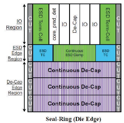
Figure 5. Physical Architecture of 16 FFC 1.8 V GPIO Library (Kuo-Hsuan Meng et al., 2017)
Similar to 40 nm and 28 nm CMOS technology nodes, 16 nm FinFet 1.8 V GPIO library uses the distributed ESD protection scheme for IO Pad-Ring construction. It has the distributed ESD clamp network with boosted triggering, between IO supply (VDDE) and common ground (VSS), as shown in Figure 6. Signals “esd_boost” and “esd_trigger” are continuous across the entire ESD edge region, and between IO and ESD edge regions. In the previous I/O libraries developed in 40 nm and 28 nm CMOS technology nodes, IO cells had both ESD diodes and ESD clamp. However, in 16 nm FinFet GPIO libraries, IO cells have only ESD diodes. ESD clamps are placed in the ESD region.
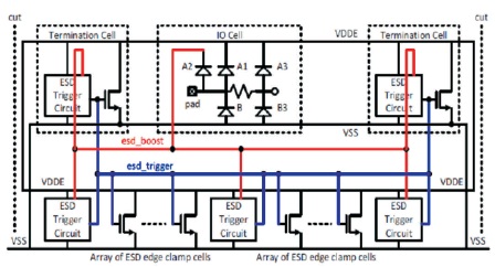
Figure 6. Distributed ESD Protection Scheme for IO Pad-Ring (Kuo-Hsuan Meng et al., 2017)
In the case of 1.8 V GPIO library, ESD clamps are built on the non-stacked DGO FinFet transistors. ESD trigger circuits are placed in the termination cells and steadily distributed in the ESD region. They are connected to the common “esd_boost” bus.
IO bank construction for 5*IO Flip-Chip (FC) Bump Template is shown in Figure 7. This IO bank uses the minimum possible repeatable segment specified for the given FC bump template. The repeatable segment includes 5 x 1.8 V GPIO cells (IO) and 1x Full-Width De-Cap Cell (D). Termination cells (T) are located in the left and right sides of IO bank.
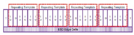
Figure 7. Example of IO Bank with the Minimum Possible Repeatable Segment for the 5*IO Flip-Chip Bump Template (Kuo-Hsuan Meng et al., 2017)
In this section, the authors compare the previously described distributed ESD protection networks implemented in 40 nm, 28 nm bulk CMOS, and 16 nm FinFet technology nodes with respect to the area of ESD components as a part of the total area of I/O cells. It is important to note that ESD design is built based on the required ESD reliability levels for HBM, CDM, and MM stresses. The results of this comparison are shown in Table 2.
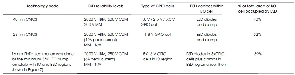
Table 2. Comparison of ESD Protection Designs in Advanced CMOS and 16 nm FinFet Processes
Note that the Machine Model (MM) ESD requirements and tests are not used for the development and qualification of I/O libraries in the resent 28 nm CMOS and 16 nm FinFet technology processes. This is because the MM test of ICs is the redundant ESD test (Duvvury et al., 2012). The ESD robustness designed into integrated circuits to survive HBM (Human Body Model) and CDM (Charge Device Model) testing provides protection against any MM-like stress. The second notice that can be done from Table 2 is that the CDM reliability level used for ESD protection design in 16 nm FinFet technology is reduced to 250 V or 6A of peak CDM current comparing to 500 V or 12 A CDM current used in previous CMOS technologies. It is necessary to maintain the area occupied by ESD components in IO cell at acceptable level around 30 40%. Otherwise, the ESD area will take more than 50% of the area of IO cell. The other reasons of CDM level reduction are discussed in the next section.
Table 2 shows that the CDM reliability level used for ESD protection design in 16 nm FinFet technology is reduced from 500 V (12 A CDM current) in 40 nm and 28 nm CMOS technologies to 250 V (6 A CDM current) in 16 nm FinFet process. Generally, there are at least two reasons for CDM level reduction in FinFet technologies. The first reason is technology specific and the second one is determined by the system level evolution of ICs in the networking industry.
The impact of technology scaling on the sensitivity of transistors and diodes to ESD stress is illustrated in Table 3.
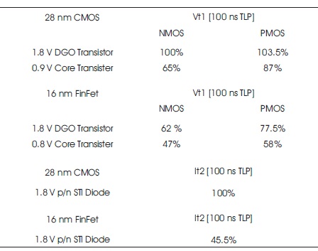
Table 3. Impact of Technology Scaling on Snapback Trigger Voltage (Vt1) and Thermal Breakdown Current (It2)
In this table, the snapback trigger voltage (Vt1) for 1.8 V DGO transistor in 28 nm CMOS process and the thermal breakdown current (It2) for 1.8 V p/n STI diodes in 28 nm CMOS process are chosen for 100%. 100 ns pulse TLP measurements show that both Vt1 and It2 parameters of devices drop significantly with the technology scaling. Transistors and diodes become more fragile under ESD events. As a result, the area of ESD devices in 16 nm FinFet technology should be much bigger to support traditional 500 V (12 A CDM current) of CDM stress compared to the 28 nm CMOS process. ESD devices can occupy more than 50% of total area of IO cells and that is impractical.
The increase of area of ESD devices in the recent FinFet technologies is not only the issue with respect to the significant consuming of silicon area in IO pad-rings. It also causes the drastic impact on the performance of high-speed IO interfaces widely used in the networking industry. The data rates for mobile networking have increased at exponential rates. For example, the data rate per lane of SERDES IO has grown recently from 8 Gbps to 28 Gbps (Wong et al., 2013). The higher data rate has also limited the capacitance on the IOs. Too much capacitance will slow down the IO data rate. Therefore, the higher data rates have maximum allowed ESD capacitance, while the large package for these devices have increased the CDM ESD current. The ESD capacitance constraints are shown in Figure 8 adopted from EOS/ESD Association.
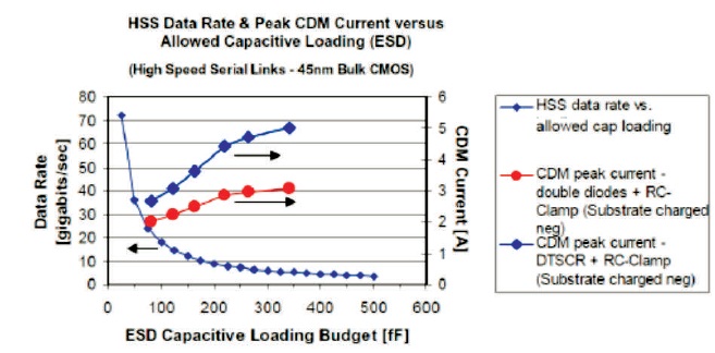
Figure 8. ESD Capacitance Budget for High Speed Serial (HSS) IO Interfaces (EOS/ESD Association)
In 16 nm FinFet technology, the performance target of SERDES IOs is 28 Gb/s. The SERDES IO pin capacitance budget for ESD (including bump) should be less than 100 fF to meet the target speed. For 250 V CDM (> 6 A), the ESD diodes connected to IO pin need to be around 400um in perimeter. This results in more than 150 fF capacitance on the IO pin just for ESD diodes. Hence, the reduced ESD protection level <250 V CDM is required in advanced FinFet technologies to support the functionality of high speed IO interfaces.
In this paper, the trends in ESD protection design in I/O libraries were analyzed for 40 nm, 28 nm bulk CMOS, and 16 nm FinFet technology nodes. It is noted, that all these I/O libraries were produced in the same FAB provider, ESD protection was built based on the common principles of distributed ESD protection networks and layouts of these I/O libraries were developed in the same I/O team with common internal layout guidelines and practices. It was shown that the developed distributed ESD protection networks provide the effective ESD solutions that can occupy just around 30-40% of total area of IO cells in spite of the CMOS / FinFet technology scaling that makes the devices significantly more sensitive to ESD stresses. The increasing of IC package capacitance driven by the higher pin counts and larger die area leads to the higher CDM peak current for a given CDM stress voltage. The higher operating frequencies cause the reduction of CDM protection level and require smaller ESD protection structures. All these factors make the ESD design more complicated in advanced FinFet technologies. The impact of technology scaling on ESD qualification target for CDM stress and the reason for its reduction were also discussed. The observed tendency is following to the ESD targets scaling previously reported by the Industry Council, ESD Association, and other chip developers (EOS/ESD Association; Qualcomm Technologies).