Figure 1. NOT Gate
Research on reversible logic gates has become one of the interesting fields in the world of electronics. This has been proved to be one of the most reliable logics that originates its place in low power CMOS skills, Nano and optical calculation and many more. These broadsheet offers the comparison of different reversible logic gates in expressions of quantum cost, delay, transistor charge, and also implementation of one of the alterable logic gates, i.e. Peres gate in a conventional half adder with the help of an efficient algorithm. The work is performed in Xilinx using Verilog coding. The simulation result shows improved efficiency, low power, and low area consumption as related to the standard half adder. This half adder can be utilized in different applications, where circuit comprising of a conventional half adder can be replaced by Peres Half Adder (HAP).
The proposed research aims to study different types of reversible logic gates and the one out of them to detect a suitable kind to modify a conventional half adder. Launder (1961) had posted the query of whether logical irreversibility is a mandatory piece of valuable PCs, disagreeing that it is, and had proved the carnal and philosophical status of this enquiry by viewing that every time a physical processor flings away material around its preceding state, it necessity produce a consistent quantity of entropy. So, a mainframe must dispel some what kTln2 of power on behalf of all bits of data it removes or else throws away. Reversible routes are those routes that fix missing information. In this study, it is found that the present irreversible machineries will disperse large amount of temperature and usually decrease life time of the winding. An irreversible processer can continually be completely reversible by taking it except whole evidence (Bennett, 1973) as loss of information results in power dissipation. Initially, in revocable circuit here must be not any fan-out, i.e., every production will be castoff individually. Then, for all input design, there would be a unique output outline. Lastly, the resultant circuit essentially is acyclic. A reversible logic track must have subsequent features:
So the chief tests of scheming reversible tracks stay lessening the quantity of gates, garbage harvests, delay, quantum charge as well as complexity. Thus, in this paper, each reversible sense gates is studied and Peres gate is chosen to design a modified half adder, on the basis of low quantum cost, delay, and transistor cost as compared to the other gates. This perfectly fits into the circuitry of HA. A Verilog code is implemented to simulate the proposed HA in Xilinx.
The n-input and k-output Boolean task f(x1, x2, x3 … xn) (denoted to as per (n, k) function) is named adjustable condition:
A circuit comprising equal amount of outputs and inputs are called reversible gates. Besides here is a single-single plotting among the path input and productions (Thapliyal & Ranganathan, 2010a; Kanth et al., 2012; Feynman, 1985). This controls the outputs from its corresponding inputs, in addition, benefits to exceptionally improve the inputs as of the outputs. The basic parameters used in reversible logic gates are mentioned below:
The types of changeable logic gates are discussed in the following subsections.
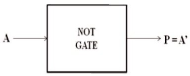
NOT gate is the first and the simplest 1x1 reversible gate. The quantum price of this gate is 0. The universal block drawing of NOT gate is shown in Figure 1 (Yelekar & Chiwande, 2011). The truth table of 1x1 NOT gate is given in Table 1.
Figure 1. NOT Gate

Table 1. Truth Table for NOT Gate
CNOT gate is a 2x2 reversible gate, also called as Controlled- NOT gate. This one is a 2x2 reversible gate. If, I and O are input and output paths, respectively, then CNOT gate can be termed as:
I = (A, B);
O = (P= A, Q= A^B)
Quantum cost of CNOT gate stays (Mamataj et al., 2014). Figure 2 displays a general diagram of 2x2 CNOT gate and its symbol. The truth table of 2x2 CNOT gate is shown in Table 2.
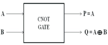
Figure 2. CNOT Gate
.jpg)
Table 2. Truth Table for CNOT Gateway
This exists as a 2x2 gate and pretended CNOT. This one is situated to effort for the fan-out drives. If A and B are inputs plus P and Q are outputs, then they are expressed such as:
P = A;
Q = A XOR B.
The quantum rate of Feynman gate (Figure 3) remains 1 (Garipelly et al., 2013). The truth table of 2x2 Feynman gate is shown in Table 3.
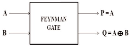
Figure 3. Feynman Gate (Garupelly et al., 2013)
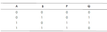
Table 3. Truth Table for Feynman Gate
It is a 3x3 gate (Figure 4) where;
Input route = I (A, B, C)
Output route = O (P, Q, R)
The outputs of a toffoli gate are:
P = A,
Q = B and
R = (A AND B) XOR C.
Toffoli gate (also CCNOT gate) bears quantum cost 5 (Peres, 1985). The truth table of 3x3 Toffoli gate is shown in Table 4.
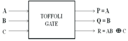
Figure 4. Toffoli Gate
Table 4. Truth Table for Toffoli Gate
This is a 3x3 gate as shown in Figure 5, where incoming data is I (A, B, C) and the outgoing data is O (P, Q, R). Then the productivity route is expressed as:
P = A,
Q = A'B XOR AC and
R = A'C XOR AB.
The quantum cost of Fredkin gate (CSWAP gate) is 5 (Thapliyal & Ranganathan, 2009). The truth table of 3x3 Fredkin gate is shown in Table 5.
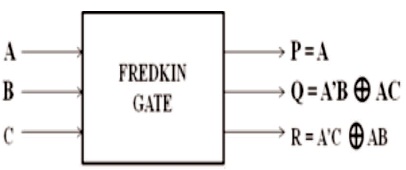
Figure 5. Fredkin Gate
Table 5. Truth Table for Fredkin GATE
This is a 3x3 gate (Figure 6). If input path is I (A, B, C) and the output path is O (P, Q, R) then, the yield is expressed as:
P = A,
Q = A XOR B and
R = AB XOR C.
The substantial rate of a Peres gate views 4 (Thapliyal & Ranganathan, 2009). The truth table of 3x3 Peres gate is shown in Table 6.
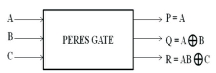
Figure 6. Peres Gate (Thapliyal & Ranganathan, 2010c)
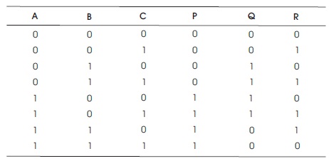
Table 6. Truth Table for Peres Gate
Too many flexible gates besides dissimilar circuits connected by these gates are conversed at this point as well as judgments are required amongst the present circuit with respect to several factors, such as quantum cost, delay, and transistor cost. Evaluation among surviving reversible gates is shown in Table 7.
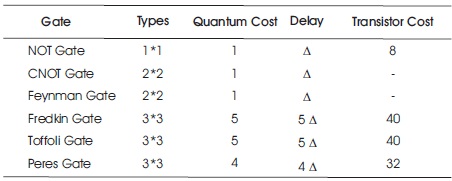
Table 7. Evaluation among Reversible Logic Gates
From the above study, it has been presented that reversible logic Peres gate bears low quantum cost, reduced delay, and low transistor charge as linked to the conventionally utilized irreversible gates. In this section, existing architecture of a half adder is discussed first, which is the standard half adder. Further, the renovated Peres gate half adder (HAP) is proposed and the improvement in different parameters is compared between the two and concluded in the other two sections of this paper.
The simple half adder consists of two 1-bit inputs and the output as sum and carry. It is designed by one XOR gate and one AND gate. The diagram of Half Adder is shown in Figure 7 and the output of half adder is realized in Table 8.
SUM = A ⊕ B;
CARRY = A & B.
The RTL view and the internal architecture of the half adder are shown in Figure 8 and Figure 9, respectively.
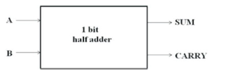
Figure 7. Schematic Half Adder
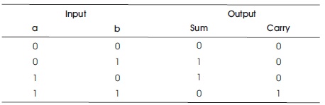
Table 8. Truth Table for Half Adder
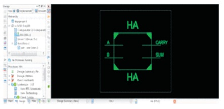
Figure 8. The RTL View of Half Adder
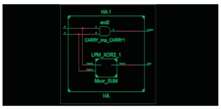
Figure 9. The Internal View of the Half Adder
The Peres Half Adder (HAP) is used for the systematic codes, where the data bits and the parity bits are kept separated. Here, a, b, c are the input parts and p, q, r are the output parts used to design the half adder. In Peres half adder, the input is assigned to p and output q shows as (sum) output of half adder and r shows as (carry) output of Half Adder.
The output of the Peres half adder is given by,
p = a
q (sum) = a ⊕ b
r (carry) = (a & b) ⊕ c
Figure 10 shows the Peres Half Adder. Table 9 displays the truth table of Peres Half adder and Figure 11 illustrates the RTL view of Peres Half Adder.
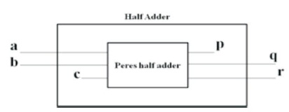
Figure 10. Peres Half Adder
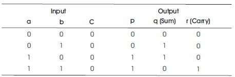
Table 9. Truth Table for Peres Half Adder
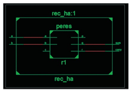
Figure 11. RTL View of Peres Half Adder
Peres Half Adder is replicated by Xilinx 13.2 in suitable Verilog codes and internal view is shown in Figures 11 and 12, respectively in which the rec-ha:1 represents Half Adder and the Peres represents the Peres Half Adder. In the representation of Peres half adder presented in Figure 10, rec_ha represents the block of half adder and the Peres represents Peres Half Adder, which is simulated using Xilinx 13.2 in suitable Verilog codes.
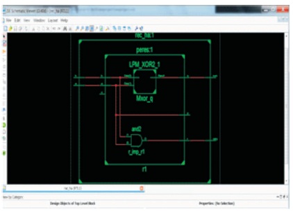
Figure 12. The Internal View of Peres Half Adder
The implementation of Peres gate is done in conventional half adder in the above section. The Verilog code is simulated in Xilinx and test bench is verified in ISIM. The appraisal table designed for the two is presented below in Table 10.
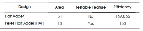
Table 10. Comparison Table
The authors thus conclude that the HAP in terms of area is more reliable than the conventional HA. The number of slices utilized in HAP is lesser than that of the HA which is responsible for the overall efficiency improvement. As we are familiar with the fact that there is a trade-off between area, power, and delay in any electronic circuitry, delay is fluctuated in the HAP, but as the area and delay product is improved, the delay can be neglected.