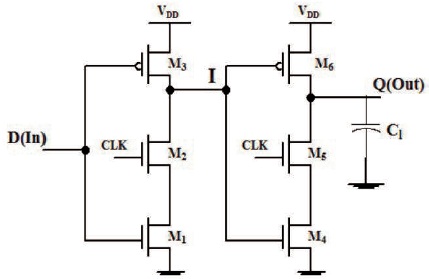
Figure 1. True Single Phased Clocked Positive Latch
In digital VLSI design, calculation of setup/hold time is a very important part. Setup/hold time defines the maximum speed of the circuit on which it can work. When a design is completed, the first step is to check the timing performances of circuit using Static Timing Analysis (STA) (Scheffer et al., 2006). Accuracy of STA depends on the data described in standard cell libraries. So accuracy of STA depends on accuracy of standard cell library characterization (Cirit, 1991; Roethig, 2003; Patel, 1990; Phelps, 1991). As the technology is scaling down, the characterization of standard cell libraries are becoming more time consuming and requires large computational time. Further due to process, voltage and temperature (PVT) variations standard cell library characterization is done for various PVT, this increases characterization greatly. In this paper, the authors present a novel approach to speed up standard cell library characterization for True Single Phase Clocked (TSPC) latch (Yuan & Svensson, 1989) setup time by developing a linear setup time model. In this model, setup time varies linearly with output load capacitance (CL) and input transition time (TR). The authors express setup time model coefficients as a function of logic gate size (Wn) of the latch. Device current/capacitance models is not used in derivation of model, so it is valid with technology scaling. Using proposed model, approximately 70% SPICE simulation during the standard cell library characterization for latch setup time can be saved. It is observed that setup time calculated using proposed model is within 2% (average) of that calculated using simulation.
Now-a-days, static timing analysis tools have made major advancements as it allows the design to be analyzed much faster. This makes it possible for a designer to experiment with different synthesis options and constraints in a short time. The accuracy of STA tools critically depends on data described in cell libraries (Dasdan et al., 2009). Latches and registers setup time calculation is prerequisite for STA (Srivastava & Roychowdhury, 2008; Gavrilov et al., 2011; Rabaey et al., 2011; Sulistyo & Ha, 2002). Now-a-days Look Up Table (LUT) is widely used with STA. In LUT approach, setup time is obtained using SPICE simulations for different combinations of CL and TR . Setup time for other values of (CL, TR) is obtained using linear interpolation. For nano-scale CMOS technologies, LUT size as well as corners increases, this increases the time for standard cell library characterization (Miryala et al., 2011). In this paper, the authors have developed a setup time model for TSPC latch as a function of TR, CL and logic gate size (Wn) of the latch. This semi-empirical model is a linear function of (CL, TR). Also they show the variation of model constants as a simple function of NMOS device size (Wn). The coefficients of the delay model using HSPICE simulations are obtained.
In this section, both data high and data low setup time model for TSPC latch is derived. Positive TSPC latch is shown in Figure 1. In this paper, setup time as data–clock offset that correspond to 5% increase in TD-Q (Delay between D and Q terminals when the latch is in transparent mode).
Figure 1. True Single Phased Clocked Positive Latch
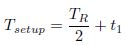
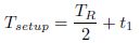
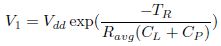
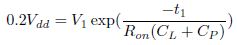
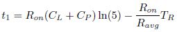
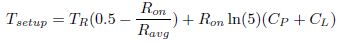
For high setup time let data input (IN) is rising from 0 to Vdd, then node I will discharge from Vdd to 0 and output node Q(out) will charge from 0 to Vdd in Figure 1. The linear transition of data input is assumed. So Vgs = (Vdd /TR) t, where Vgs is gate to source voltage of NMOS transistor M1, Vdd is the power supply voltage, and t is the time. When latch is in transparent mode, CLK is Vdd. For latch, setup time is the minimum time for which the input data D to be stable before the latching edge of the clock (in this case it is the falling edge). So for TSPC latch, the node I must discharge from Vdd to 0.2 Vdd before falling edge of clock. This ensures that transistor M6 in Figure 1 is ON and there is no need of clock after this because output node Q(out) will charge toward Vdd through M6. 0.2 Vdd point for node I is used, because it is observed that time taken by node I to discharge from Vdd to 0.2 Vdd is enough for Q(out) node to settle down. The node I discharge comprises of two regions: first when input D(IN) is switching from 0 to Vdd and region 2 when input is stable at Vdd. In region 1, input rises from 0 to Vdd in transition time TR and node I discharges from Vdd to V1. Let node I takes t1 time to discharge from V1 to 0:2 Vdd. So setup time is equal to
Assumption 1: During input transition from 0 to VD, the transistors M1 and M2 remain in linear region. This assumption is based on the fact that capacitance at node I is very low. Therefore, node I discharges quickly and drain voltage of M1 remain low. Using the above assumption,
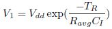
In equation (2), Ravg = Ravg; NMOS1 + Ravg; NMOS2 and CI is capacitance at node I, which is given as C1 = CPI + (Cload ||Cp), where CP and CPI are parasitic capacitance at load output node and intermediate node (I), respectively in Figure 1 (both are proportional to Wn (Wp)). Since, node I discharge from Vdis to 0:2VD in time Tdis .
Therefore,
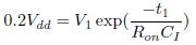
In equation (3),Ron = Ron;NMOS1 + Ron; NMOS2 . Using equations (2) and (3) we have,
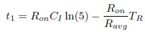
Substituting (4) in (1) we have,
Now according to value of Cload , there are two cases
Case I: When Cload ≪ CP
This implies Cload ||CP = Cload using equation (5).
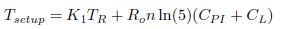

The model coefficients K1, K2 and K3 can be obtained by fitting the model in the HSPICE simulated data. From equation (8), it can be clearly seen that K2 is inversely proportional to Wn.
But K1 and K2 are independent of Wn.
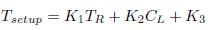
Case II: When Cload >> CP.
This implies Cload ||Cp = Cp.
Using equation (5).
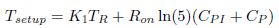
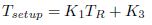
From equation (10), it can be seen that setup time remains constant for higher values of Cload. The model coefficients K1 and K3 are independent of Wn. While, the setup time Ts is independent of Cload.
All these observations will be validated in next section.
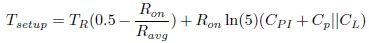
For low setup time let data input (IN) is switching from VD to 0, then node I will charge from 0 to VD and output node Q(out) will discharge from VD to 0 in Figure 1. We assume linear transition of data input. For this case, output node Q(out) must discharge from VD to 0:2VD before falling edge of clock otherwise after falling edge of clock transistor M5 in Figure 1 will be OFF and there will be no path for output to discharge. 0:2VD for Q(out) node is used, because it is observed that after reaching 0:2VD point, there is less impact of variation at node I on Q(out) node. Let during input switching, output node Q(out) has discharged from VD to Vdis and it takes Tdis time to discharge from Vdis to 0:2VD. So setup time is equal to,
Assumption 2: During input transition VD to 0, the NMOS transistor M4 remain in linear region.
The output node Q(out) discharge comprises of two regions: first when input D(IN) is switching from VD to 0 and region 2 when input is stable at Gnd. In region 1, input switch from VD to 0 in transition time TT and output node Q(out) discharges from VD to Vdis . Using the above assumption,
In equation (12), Ravg = Ravg;NMOS4 + Ravg;NMOS5 .
Now let node Q(out) discharge from Vdis to 0:2VD in time Tdis.
So,
Now using (12) and (13).
Substituting (14) in (11),
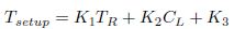
The model coefficients K1 , K2 , and K3 can be obtained by fitting the model in the HSPICE simulated data. From equation (16) it can be clearly seen that K2 is inversely proportional to Wn. But K1 and K3 are independent of Wn. All these observations will be validated in the next section.
In this section, the results are validated using HSPICE simulations. Also coefficients of equations (8), (10), and (16) are extracted using the simulation data. The authors use a 45 nm Predictive Technology Model (PTM) (Predictive Technology Model, 2011) CMOS files in these simulations. An ideal clocks with period 400 ps is used in these simulations. In all figures points are simulated data and dotted lines are model equations.
Figure 2 (a) shows the variation of data high setup time with TR at constant CL. Figure 2 (b) shows the variation with CL at constant TR. These figures show that the setup time model equations (8) and (10) fits well on simulated data. Figure 2 (b) verifies our observation that data high setup time varies linearly with CL for lower values and remain approximately constant for higher values of CL. Figure 3 verifies the observations that data high setup time model coefficients k1 and k3 are independent of Wn. Figures 4(a) and 4 (b) show the variation of data low setup time with CL at constant TR and with TR at constant CL, respectively.
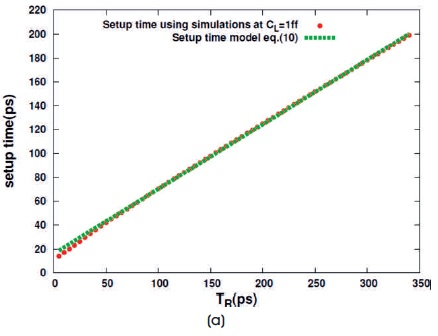
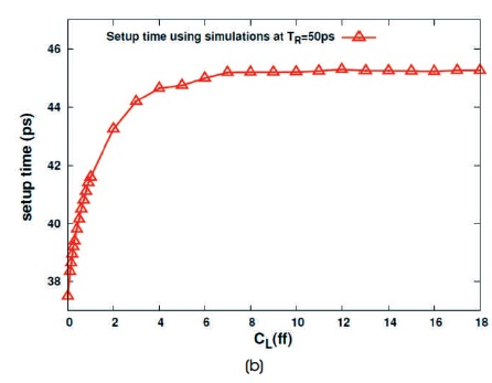
Figure 2. Variation of Data High Setup Time for TSPC Latch
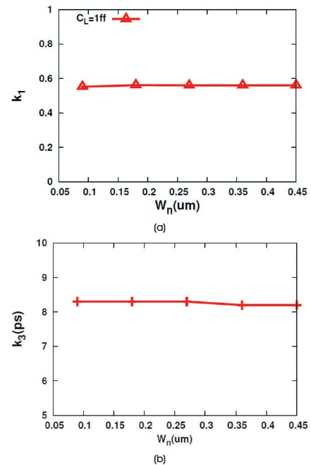
Figure 3. Variation of Data High Setup Time Contants with Wn for TSPC latch
These figures show that the data low setup time model (16) fits well on simulated data. Figure 4 (a) verifies the observation that data low setup time varies linearly with CL. Moreover, in Figure 5, it is shown that the model coefficient K1 does not vary with the Wn, which is also consistent with this model (15).
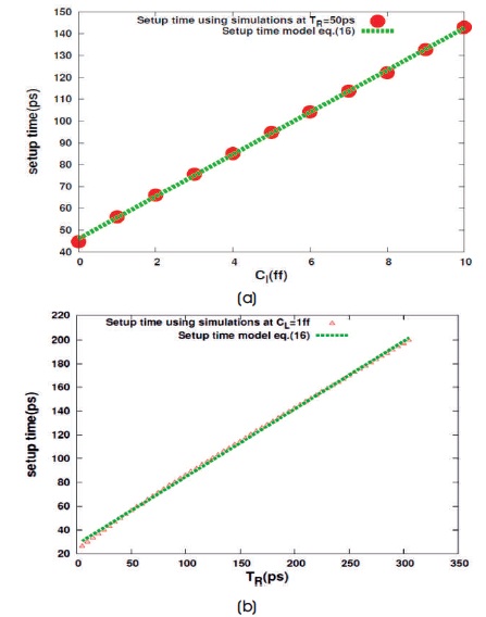
Figure 4. Data Low Setup Time Variation for TSPC Latch
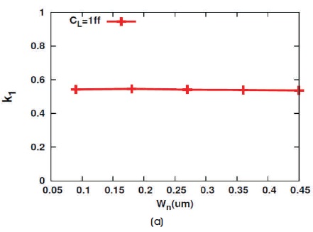
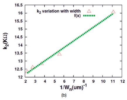
Figure 5. Data Low Setup Time Constants Variation with Wn for TSPC Latch
In this paper, the authors have presented a setup time model for TSPC latch in which setup time varies linearly with TR and CL. The relation of the setup time model coefficients with transistor size Wn (assuming that the ratio of its NMOS and PMOS devices remains constant. Wp =2Wn) is also derived. To derive these relations, device currents/capacitances models are not used. The authors have used the topology of the gate and the charging/discharging phenomenon of the load stage. Therefore, these relations are general in nature and would not change with technology scaling. Model constants from simulated data are extracted. It is shown that extracted coefficients from simulated data vary according to derived model coefficients. By using this model, one can save the precious time and number of simulations during standard cell library characterization. As a future work, it would obtain the relation of setup time model coefficients with PVT variations and also work on stress effect on this setup time model.