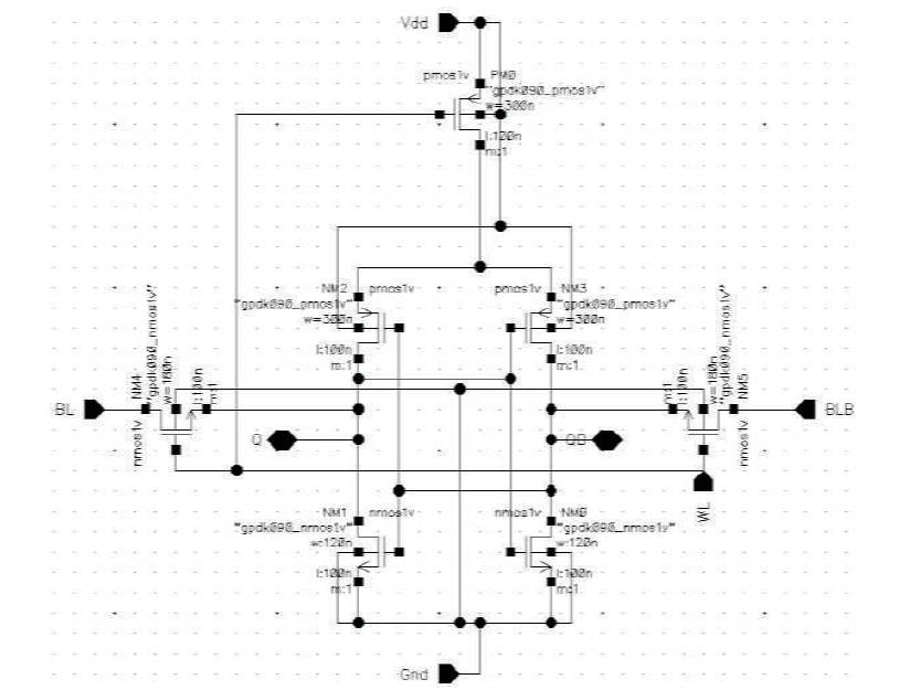
Figure 1. 7T SRAM bit-cell
In today's smart digital world, for any digital circuit, one of the most vital parts is Static Random Access Memory (SRAM). The power consumption, speed, area etc. have been the major areas of concern in the evolution of different memory architectures. Researchers are working on the modification of basic 6T SRAM cell to meet their requirements by optimizing the performance parameters of SRAM. In the present research work, a novel 7T SRAM cell has been designed, having both low latency and low power. The proposed design has allowed control over threshold voltage and reduced the leakage current. As a consequence, there is a reduction in the static power consumption and load capacitance of SRAM. Dynamic power consumption, Static power consumption, Unit cell delay, Power Delay Product (PDP), Static Noise Margin (SNM) and Write SNM are estimated for 6T and 7T for comparison. On comparison of the performance parameters, the proposed 7T SRAM cell was found to be the cell with least power consumption along with lowest latency among the two cells. Most of the compared parameters show an improvement in the performance of the proposed design as compared to the regular 6T configuration of SRAM. This research was carried out using Cadence Virtuoso Tools on 90 nm technology with Assura Verification tool and Spectre simulation tool.
World over the trend is towards handheld devices which are internet enabled (Sumi and Ranga, 2016). Advances in silicon technology have made possible the design of Very Large Scale Integration (VLSI) chips which has made the handheld device possible . These devices have specific requirements for optimal usage of power. Minimum energy operation for digital circuits requires scaling the power supply below the device’s threshold voltage (Verma et al., 2008). SRAMs are the most important part of any handheld device (Rabaey et al., 2002). The amount of power consumed by SRAM is the major component of the total power consumed by the whole device (Onsori et al., 2016). Hence a SRAM (Page and Thorsteinsson, 2010) designed with power-optimized design is the focal point of many research works (Aly and Bayoumi, 2007). The all perfect SRAM design is still an elusive concept (Kurdahi et al., 2006). In this paper, an effort is made to design a high speed and low power 7T SRAM bit cell. The proposed design is implemented and simulated using Cadence virtuoso tools with 90 nm generic process design kit with proper aspect rations being used for transistors.
SRAMs are essential components of handheld devices (Sumi and Ranga, 2016). They are the major contributors to the power consumption of a device. Hence the battery life is majorly determined by the amount of power consumed by the SRAM memory block of the chip (Rabaey et al., 2002). If the power consumed by SRAM is optimized by adopting innovative design methods, then the battery life will increase due to the reduction in the power consumption of SRAM . Hence the majority of research in SRAM is in optimizing the bit cell for reduced power consumption, without compromising on the performance of the SRAM (Aly and Bayoumi, 2007). This study is directed towards the reduction of the power consumed, without compromising on the stability and access speed of the memory cell. Complementary Metal Oxide Semiconductor (CMOS) technology is used because of the inherent low static power consumption property of the technology. Power consumption is majorly due to switching and leakages in standby mode (Fallah and Pedram, 2005). The architecture of the memory cell chosen is 7T. The cell is implemented using Cadence virtuoso tools with 90 nm generic process design kit with proper aspect ratios of transistors. 7T is chosen as the right choice based on the intentions to attain high density for SRAM with better performance characteristics. Higher transistor count will consume more silicon area. Lower transistor count in the bit cell, though provides higher memor y density will have poorer performance characteristics. Hence to have best of both, the world’s 7T architecture was chosen for the proposed work. An extra p-channel Metal Oxide Semiconductor (pMOS) transistor has been added to the basic 6T SRAM cell to get 7T bitcell. The seventh transistor is introduced with the intention of reduction of dissipation of power in the device as well as controlling the supply of the cell. This extra PMOS will control the triggering of the cell with control on subthreshold leakage and the threshold voltage of the device.
An extra PMOS transistor has been added to the basic 6T SRAM cell to get 7T bit-cell. Figure 1 shows the 7T bit cell for SRAM.
Figure 1. 7T SRAM bit-cell
The working of the SRAM bit cell under various modes of its operation is explained below.
During a ‘read’ operation, the bit lines (BL and BLB) are precharged to VDD and then Word Line (WL) signal is asserted high. Depending on the data stored (Low/High) at the nodes Q and QB, one among the NMOS transistors of cross-coupled inverters will start conducting. Next, discharging of bit lines occurs through the respective access transistors to NMOS transistors of inverters to Ground (GND). The data stored is then interpreted by sensing the potential difference between the nodes with the help of sense amplifier. The signal applied on the extra transistor inserted in pull up provides the supply path with the varied threshold and lowered leakage.
During a ‘write’ operation, the Word Line (WL) signal is increased to VDD . Further the access transistors are turned ON. Also, the signal applied on the extra transistor inserted in pull up provides the supply path with the varied threshold and lowered leakage. Let’s proceed with the assumption that node Q is stored with high logic and low logic at QB node. In order to write the high logic at QB node and low logic at Q node, bit lines BLB and BL are supplied with high and low logic respectively with the help of write driver circuitry. The data stored at Q node will get discharged through the respective access transistor by bit line BL. Concurrently, the data stored at node QB is pulled up to VDD through the respective transistor by bit line BLB.
In order to perform hold operation, the Word Line (WL) signal is pulled down to GND. As a result, the access transistors go into an OFF state. Also, the extra transistor inserted in pull up is tuned ON. But this PMOS transistor passes a lesser voltage than VDD to the back to back inverters. This is due to the ON resistance of PMOS. Hence this will result in a significant reduction in the leakages and static power consumption of the bit-cell occurring during the hold state.
Stability analysis of bit cell gives an idea regarding how robust the design of the cell is. The characterization of designed SRAM cell has been performed using its stability analysis. In the design process of SRAM cell, one of the most significant functional constraints is its retention of the data both in the hold and access modes. Scaling results in increased leakages and variability. Scaling also lowers the supply voltage. All the above-mentioned factors become root cause to the reduction of stability of SRAM cell. The stability is generally given by Static Noise Margin (SNM). SNM is the maximum value of the constant noise voltage level which can be withstand by the designed cell in order to maintain the stored data bit. Hence, stability of SRAM cell is its ability to hold a stable state. This is also defined as the peak value of the noise which can be inhibited by the cross-coupled inverter circuitry before their state alteration.
The standard 6T SRAM is used for the comparison with the proposed 7T . The performance matrices chosen for comparison are dynamic power consumption, static power consumption, unit cell delay, Power Delay Product (PDP), Read Static Noise Margin (SNM), and Write SNM. This modification to 6T SRAM bit cell has resulted in enhancement of many performance parameters. The performance matrix is used to compare the performance of the proposed bit-cell with the standard 6T bit-cell. The results are tabulated in Table 1.


Table 1. Comparison Parameter Matrix for 6T and 7T
The reference SRAM cell 6T and the proposed SRAM cell 7T were designed and simulated using Cadence Virtuoso Tools with 90 nm generic process design kit and were simulated at 1 GHz frequency (Verma et al., 2008) . The SRAM cells are designed with assisting circuits like write assist circuit, read assist circuit, sense amplifier, precharge circuit etc. Along with this, a capacitor of 0.1 fF was used as load in order to realize the charging and discharging of bit cell.
Both 6T and 7T were implemented and simulated for comparison. The results from the simulation are tabulated in Table 1. From the results, the following observations are made. The dynamic power consumption has reduced by 57%, and the static power consumption has decreased by 55.23%. This results in attaining higher chip densities, longer battery life, lower cooling cost and packaging costs. The unit cell delay has reduced by 31.655%; this facilitates faster memory chip designs. The SNM has increased by 6.928%, hence there is an improved stability of the bit-cell. The write SNM has decreased by only 2.366%.
The proposed design is implemented and simulated using Cadence virtuoso tools with 90 nm generic process design kit with proper aspect rations being used for transistors and was simulated at 1GHz frequency. From the performance matrix chosen for comparison between the 6T and the proposed 7T, it can be seen that there is a significant improvement in the performance characteristics of the proposed 7T. The addition of an extra transistor has yielded many benefits.