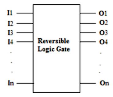
Figure 1. Schematic of Simple Reversible Logic Gate
Reversible Logic is the dominating field of research in low power Very-Large-Scale Integration (VLSI). In recent time, reversible logic has gained special attention in order to reduce power consumption mainly in concern to digital logic design. The main aim of this paper is to realize and synthesize shift counters like Ring counter and Johnson ring counter using reversible logic. Shift Counter is a sequential circuit that performs counting through shifting operation in a loop fashion. The output of last register of the circuit will be fed to the input of first register. Ring counter owns its applications in clock division circuits, square wave generators, hardware logic design of Application-Specific Integrated Circuit (ASIC) and Field Programmable Gate Array (FPGA) circuits etc., Ring counter and Johnson Ring counter are designed using reversible logic to reduce power dissipation. A Boolean function f (i1 , i2 , i3 , ……, in ) having 'n' inputs and 'm' outputs is said to be logically reversible, if the number of inputs are equal to the number of outputs ( i.e. n = m) and the input pattern maps uniquely to the output pattern. Few reversible logic gates present in the literature are NOT gate, Feynman Gate (CNOT gate), Double Feynman Gate, Peres Gate, TR gate, Seynman Gate etc. The reversible gate must run both in forward and backward directions such that the inputs can be retrieved with the knowledge of outputs. The two limitations of logical reversibility are Fan-out and Feed-back are not allowed. Signals from required output lines are duplicated to desired lines using additional reversible combinational circuits to overcome the Fan-out limitation. Reversible Logic has applications in various fields like Quantum Computing, Optical Computing, Nanotechnology, Computer Graphics, Low power VLSI etc. Reversible logic has gained essence in recent years largely due to its property of low power consumption and low heat dissipation. In this paper, shift registers like shift right register and shift left register which have less heat dissipation and low power consumption is proposed. Till date, shift counters are not yet designed using reversible logic. In this paper, an attempt has been made to design shift counters like ring counter and Johnson ring counter using reversible logic. The designed circuits are analysed in terms of Quantum Cost (QC), Garbage Outputs (GO) and number of gates. The circuit has been designed and simulated using Xilinx software.
When logical computations with minimal energy dissipation are considered, logical reversibility plays a fundamental role. It was proved that reversible logical computation has a distinctive feature that it conserves information bits instead of erasing those bits. Power (Rabaey & Pedram, 2012) is an important factor to be considered along with time delay and area. The power consumption/heat dissipation will be very less in reversible circuits when compared with the irreversible logical circuits. According to Landaurer’s (1961) principle, easing of each bit of information causes KTln2 Joules of heat dissipation, where K is Boltzman constant which is equal to 1.3805 x 10⁻²³ J/T and T is temperature. He proved that heat dissipation is not due to the process undergone in logical computation. It is due to wiping of bits in the process. This heat dissipation may be very small if a single information bit is considered, but in very high complex VLSI circuits where large numbers of transistors are placed on a single chip, this type of wiping of bits occurs at large amounts. It is predominant to understand that there is a direct relationship between the number of bits lost to the amount of heat dissipation. Later Bennett (1973) and Bennet (1988) proved that this type of heat dissipation can be reduced through logical reversibility. Quantum logic gates are used to design reversible quantum circuits . Bennett argued that KTln2 joules of energy dissipation can be prevented if the logical computation is done using logical reversibility. Logical computation using reversible logic doesn't require erasing of information bits. This paper mainly concentrates on the realization of Ring counter and Johnson Ring counter using logical reversibility.
The practical limitation for high performance chips is heat dissipation. According to Moore's law, the number of transistors integrated over the chip must be doubled every year as the chip size reduces to half. VLSI has already reached nanometer technology and the researchers are predicting that the road map of Moore's law will no longer gets satisfied since the size of the transistor cannot be reduced further without falling into the leakage problems. Therefore the operating voltage levels cannot be scaled down than current levels. Hence reversible computation gives an interesting solution that if the information bits are left without erased, improvement of energy efficiency is possible. The conserved information bits are left un-computed. The importance of reversible computation cannot be ignored, even though the hardware complexity increases with it. With reversible computation, energy dissipation / consumption can be reduced or even can be eliminated if computation becomes information loss less.
The reversible computing involves the use of reversible gates which consists of the same number of inputs and outputs i.e., there should be one to one mapping between input vector lines and output vector lines. In reversible computation, the reversible gates are made to run both forward and backward directions(Bennett, 1973) . If the device obeys both the above two conditions, it satisfies the second law of thermodynamics which preserves the information bits without getting erased and guarantees no heat dissipation and less power consumption. Certain limitations are to be taken into account when designing circuits based on reversible logic.
In reversible computation using outputs, one can obtain the full knowledge of inputs. To overcome the Fan-out limitation, the output lines are duplicated into required number of lines that are required to drive the inputs of the consecutive device by using additional reversible combinational circuits. Similarly, to overcome Feed-back limitation, delay elements are used. There are few cost metrics associated with logical reversible computation (Feynman, 1985; Peres, 1985; Rangaraju et al., 2010) They are Garbage outputs Number of gates, Quantum cost Constant inputs which are used to estimate the performance of reversible circuits (Thapliyal and Ranganathan, 2010) Garbage outputs are the extra outputs which help to make inputs and outputs equal in number in order to maintain logical reversibility. They are left ideal without performing any operation. Number of gates count will not be a good metric since more number of gates can be brought together to form a new gate. Quantum Cost is the number of elementary or primitive gates (or CNOT and NOT Gates) required to implement a reversible logic gate. It is nothing but the number of reversible gates (1×1 or 2×2) required to construct the circuit. The quantum cost plays a prominent role in logical reversible computation. If the quantum cost is more, then the area under the circuit increases, which increases the propagation delay. But quantum cost doesn't impact heat dissipation. Delay is one of the important cost metrics (Thapliyal and Ranganathan, 2010) reversible circuit design can be modelled as a sequence of discrete time slices, and depth is the summation of total time slices.
The schematic of reversible logic gate which contains same number of inputs and outputs is shown in Figure 1 . The basic reversible logic gates present in the literature are mentioned and a short notes on each gate is given below. The reversible logic gates which are suitable for the desired design are considered. The reversible logic gates present in the literature are NOT Gate, CNOT or Feynman Gate (Feynman, 1985), Double Feynman Gate (Feynman, 1985), Toffoli Gate (Toffoli 1980), Fredkin Gate (Shende et al., 2003), Peres Gate (Peres, 1985), TR Gate (Peres, 1985) etc., Among all the above listed reversible logic gates, NOT Gate is a 1×1 reversible logic gate which is basically an elementary gate. It just complements the given input and shifts it to the output. CNOT gate is a 2×2 reversible logic gate which is also a preliminary elementary gate. CNOT gate is also called as Feynman Gate. The quantum cost of CNOT Gate is 1. These NOT and CNOT gates are the basic primitive gates which are involved in the realization of new reversible logic gates. The CNOT gate is used to duplicate a single line into two duplicate lines as reversible logic does not allow fan-out.
Figure 1. Schematic of Simple Reversible Logic Gate
The schematic and truth tables of both NOT Gate and CNOT gate are shown in Figures 2 and 3, and Tables 1 and 2, respectively.
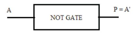
Figure 2. NOT Gate

Table 1. NOT Gate Truth Table
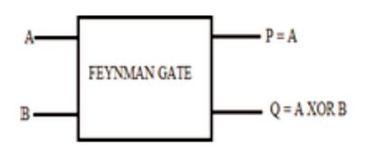
Figure 3. CNOT Gate
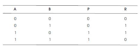
Table 2. CNOT Gate Truth Table
There are different types of 3×3 reversible logic gates. The output vector O (P, Q, R) of each reversible logic gate is defined as the function of input vector I (A, B, C) as shown in Figures 4 to 8 and the respective truth table of every reversible logic gate is depicted in Tables 3 to 7, respectively.
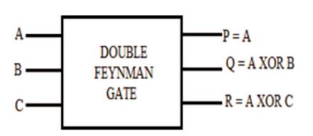
Figure 4. Double Feynman Gate
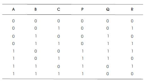
Table 3. F2G Gate Truth Table
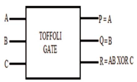
Figure 5. Toffoli Gate
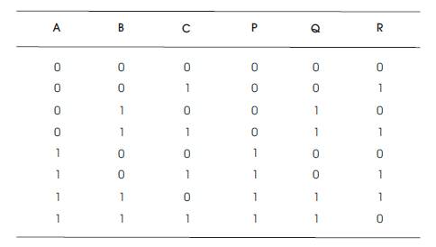
Table 4. Toffoli Gate Truth Table
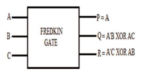
Figure 6. Fredkin Gate
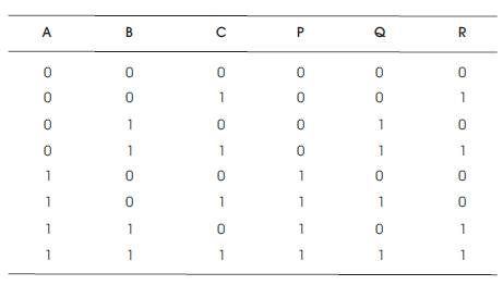
Table 5. Fredkin Gate Truth Table
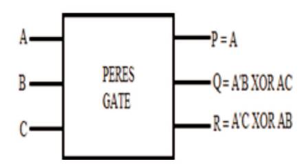
Figure 7. Peres Gate
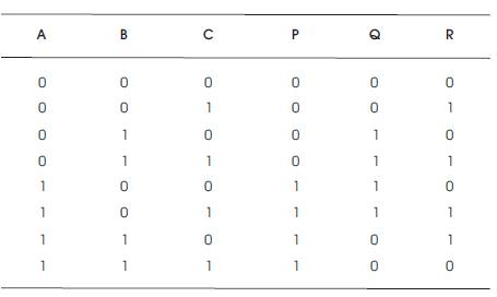
Table 6. Peres Gate Truth Table
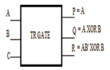
Figure 8. TR Gate
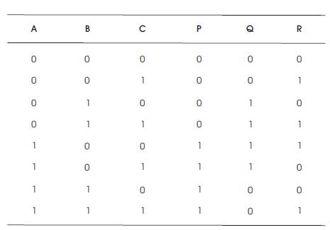
Table 7. TR Gate Truth Table
The Quantum Cost of F2G Gate is 2
The Quantum Cost of Toffoli Gate is 4.
The Quantum Cost of Fredkin Gate is 5.
The Quantum Cost of Peres Gate is 4.
The Quantum Cost of TR Gate is 4.
In concern with the circuit requirements, the basic gates like AND Gate and OR Gate can be realized using reversible logic gates as shown in Figure 9. The 'R' output of fredkin gate gives the AND gate operation when it's 'C' input is driven with 0. Similarly the 'Q' output of fredkin gate gives the OR gate operation when it's 'C' input is driven with The realization performed is shown in Figure 9.
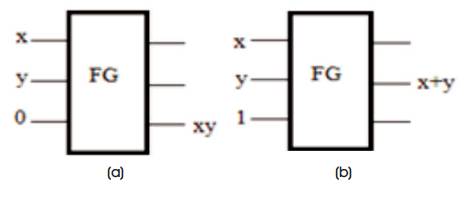
Figure 9. (a) AND Gate using Fredkin, (b) OR Gate using Fredkin
Similarly a multiplexer can also be realized using a Fredkin Gate. The reversible multiplexer designed using fredkin gate is shown in Figure 10.
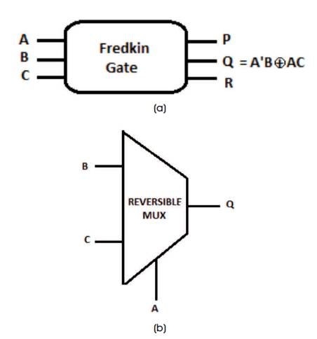
Figure 10 (a & b). Fredkin Gate Realized as 2×1 Multiplexer
The 'Q' output of fredkin gate gives the minterm expression of 2×1 multiplexer, if 'A' input of fredkin gate is considered as selection line and 'B', 'C' inputs are considered as inputs lines. 'P', 'Q' lines are left ideal without usage. These are termed as garbage outputs. Here fredkin gate is considered to realize multiplexer because it gives better performance with acceptable Quantum Cost. In general D Flip-flop is used to design shift registers. The block diagram of D-FF and its truth table are shown in Figure 11 and Table 8 respectively. The characteristic equation of DFF is given as,
Q(t+1)= D
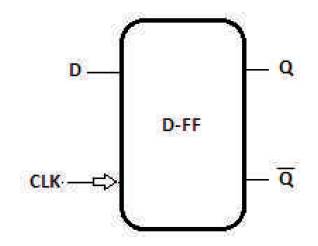
Figure 11. D Flip-flop

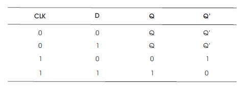
Table 8. Truth Table of D Flip-Flop
The excitation table of D-FF is shown in Table 9. Excitation table gives the knowledge of inputs from possible combinations of outputs.
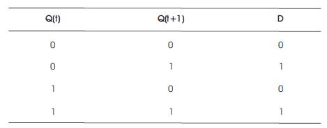
Table 9. Excitation Table of D Flip-Flop
A minterm expression can be written for D as a function of Q (t) and Q (t+1) from Table 9.
D=Q(t)
In order to realize a D flip-flop using suitable reversible logic gates, the minterm expression (2) is considered. Here a fredkin (F) gate and CNOT gate or Feynman gate is used to realize a reversible D Flip-flop. Feynman Gate (FG) is used to overcome feedback limitation of reversible logic.
The proposed D Flip-flop using reversible logic is shown in Figure 12.
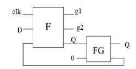
Figure 12. Proposed Reversible D Flip-flop
In the existing literature (Syamala and Tilak, 2011; Thapliyal and Ranganathan, 2010; Rajmohan & Ranganathan, 2011; Shende et al., 2003; Garg & Saini, 2014; Mamataj et al., 2014; Mamataj & Das, 2014; Santhiya and Kumar, 2014; Das et al., 2016; Majumdar & Saini, 2015; Singh & Pandey, 2016), flip-flops and latches are designed using different types of reversible logic gates like RSJ Gate, Seynman Gate (Garg & Saini, 2014), RM Gate (Rajmohan & Ranganathan, 2011) etc. In this paper, an attempt has been made to realize D Flip-flop using basic reversible logic gates like fredkin and CNOT gate, which are further used to design Shift registers like shift right register, shift left register and Shift counters like Ring Counter, Johnson Ring counter etc. The block diagrams of different 4-bit shift registers and 4-bit shift counters using reversible logic are depicted in Figures 13 to 16.
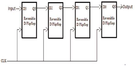
Figure 13. Proposed Shift Right Register using Reversible D Flip-flop
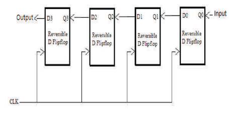
Figure 14. Proposed Shift Left Register using Reversible D Flip-flop
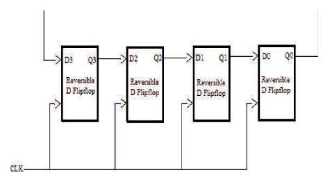
Figure 15. Proposed Ring Counter using Reversible Logic
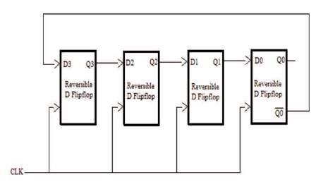
Figure 16. Proposed Johnson Ring Counter using Reversible Logic
The D flip-flop proposed using reversible logic in Figure 12 is used to design the circuit. The reversible logic gates selected in realizing the above shift registers are of minimum quantum cost with optimistic performance.
The RTL schematic of proposed D-FF using reversible logic is shown in Figure 17. From Figure 18, it is very clear that every clock data given at the input end gets transferred to the output terminal. Hence, the D flip-flop operation takesplace. The simulation results of shift registers like shift left and shift right register using reversible logic are depicted in Figures 19 and 20, respectively.
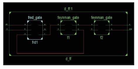
Figure 17. RTL Schematic of Proposed D-FF using Reversible Logic
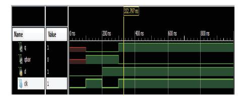
Figure 18. Simulation Output of Proposed D-FF using Reversible Logic
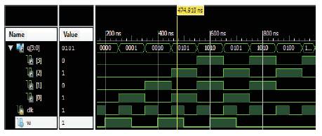
Figure 19. Simulation Output of Proposed Shift Left Register using Reversible Logic
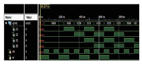
Figure 20. Simulation Output of Proposed Shift Right Register using Reversible Logic
From the simulation outputs in Figures 19 and 20, it can be clearly noticed that for every input clock pulse, the shifting operation is performed.
The simulation results of shift counters like ring counter and Johnson ring counter using reversible logic are depicted in Figures 21 and 22, respectively. From Figure 21, it can be clearly noticed that high value is getting shifted which is generally a ring counter operation. From Figure 22, the twisted operation of high value is clearly seen which is Johnson counter's operation basically. The simulation output of ring counter and twisted ring counter on FPGA is shown in Tables 10 and 11, respectively.
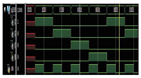
Figure 21. Simulation Output of Proposed Ring Counter using Reversible Logic
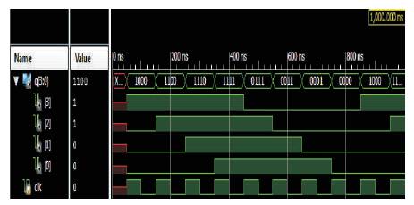
Figure 22. Simulation Output of Proposed Johnson Ring Counter using Reversible Logic
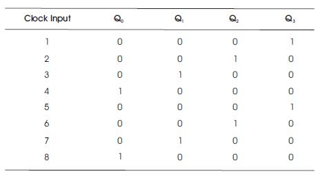
Table 10. Simulation Output of Proposed Ring Counter using Reversible Logic on FPGA
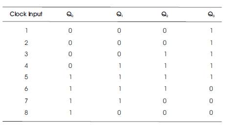
Table 11. Simulation Output of Proposed Johnson Ring Counter using Reversible Logic on FPGA
In Table 12 different reversible logic gates used to build flip-flops are listed along with their Quantum Costs (QC). Table 13 gives the comparison of proposed D-FF using reversible logic with existing models. The quantum cost of the proposed DFF is less when compared with the remaining existing models. The gates that were used to design DFF in each existing and proposed models are listed along with their respective quantum cost, garbage outputs and constant inputs. It is very clear that the proposed DFF's quantum cost is less which in turn possesses less propagation delay.
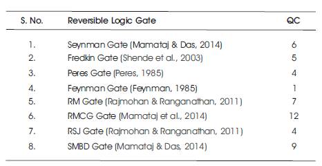
Table 12. Different Reversible Logic Gates with their QC
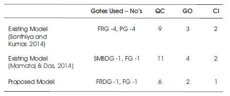
Table 13. Comparison of Proposed D-FF with Existing Models
Table 14 gives the comparison of reversible shift registers and shift counters.
It is very clear that the quantum cost of every proposed reversible shift register is reduced when compared with the existing circuits. Hence the quantum cost is reduced, and the garbage outputs were also reduced wherever it is possible. In current literature, the shift counters are not built using reversible logic. In this paper, an attempt has been made to design shift counters using reversible logic. The quantum cost and garbage outputs of that particular shift counter are mentioned in Table 14. The comparative study of reversible and irreversible circuits in terms of its Propagation Delay is given in Table 15.
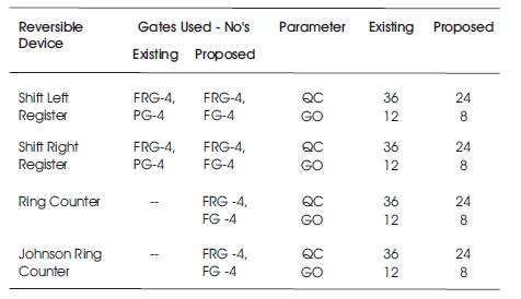
Table 14. Comparative Study of Reversible Shift Registers and Shift Counters
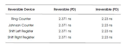
Table 15. Comparative Study of Reversible and Irreversible Circuits
Earlier in this research (Naguboina & Anusudha, 2017a, 2017b; Anusudha & Naguboina, 2017; Naguboina & Anusudha, 2018), different digital circuits are realized using reversible computation. In this paper, the proposed shift registers and shift counters using reversible logic is designed with minimum quantum cost and garbage outputs. In general, the propagation delay is slightly more in reversible logic circuits when compared with the irreversible logic circuits. But it will be really an achievement, if the propagation delay was reduced using reversible logic circuit than the irreversible circuits. In the existing models, flip flops are designed using derived reversible logic gates in which quantum cost is more whereas the flip flops proposed are designed using basic reversible logic gates with minimum quantum cost. These flip flops are used in shift registers and shift counters, in which quantum cost is reduced when compared with existing models.
The designed circuits are simulated and analysed in terms of propagation delay. If the quantum cost and garbage outputs are more, then it is clear that the area of the circuit increases which in turn increases propagation delay also. It is observed that the propagation delay of reversible circuits is slightly higher than the irreversible circuit which is negligible. This can be termed as disadvantage of these designs. Despite of this demerit, the importance of reversible circuits cannot be neglected because of its efficiency in terms of heat dissipation. Eighty percentage of heat efficiency can be obtained by using reversible logic
The future scope is, the circuits that are designed can be implemented more precisely with less quantum cost and less garbage outputs, so that the propagation delay and area can also be reduced.