Figure 1. Read and Write Static Noise Margin on Different Technologies (Jiao et al., 2016)
In this paper, various Low Power SRAM cell design techniques have been reviewed on the basis of power, stability, and delay. Many studies have proposed various SRAM architectures for different applications. It has been reported that 6T SRAM cell are high in speed but at low supply voltage, stability is a critical issue. It is found that 8T SRAM cell shows the highest level of stability at low supply voltage, but it has area penalty. Hence in this work all the required performance parameters of various SRAM cell architectures have been reviewed. This work will be helpful for VLSI designer to choose proper memory architecture as per applications. For example, machine learning needs high performance memory block while bio-medical implants require low power memory block. This paper also presents various tradeoffs between various design parameters of SRAM.
SRAM is a type of memory, which is used to make on-chip cache memories for microprocessors in electronic devices. “The use of SRAM on Intel products varies by market segment from about 10% to around 50% of the die area”, quoted Kaizad Mistry, Vice President and Director of logic technology integration at Intel. Both dynamic and static memories can be used in computer, but there is a cost difference between them. The static memory stores data in flip flop, while dynamic memory stores data as a charge on capacitor. But the charge on capacitor has to be periodically refreshed for every cycle. This is the major drawback of using dynamic memory (Hoffmann, 1982).
SRAM cell structure consists of two back to back inverters and two pass transistors. The inverters form the feedback loop stabilizes the state of memory. The pass (access) transistors are used for read and write operation to pass the value through / into bitline (Kang and Leblebici, 2003).
The basic SRAM cell consists of 6 transistors. The input of one inverter is an output of another inverter. During read operation, the bitlines should be precharged and for write operation, bitline passes the data into bistable circuitry. In hold operation, access transistors remain in OFF condition. A 6T CMOS SRAM cell is the most popular SRAM cell due to its superior robustness, low power, and low-voltage operation (Khare et al., 2008).
The low power design means to prevent circuits from the excessive leakage of current. But the circuit cannot satisfy all the requirements of parameters at a time. For example, if power dissipation goes low, then stability or speed can go high. There are two types of power dissipation, viz., static power dissipation and dynamic power dissipation. Static dissipation is due to leakage current, which flows from power supply to ground in sleep mode, whereas dynamic power dissipation is due to charging or discharging of load capacitance and short circuit current. Also, there is another short circuit current that exists, which contribute to increased power dissipation like reverse biased of a diode, sub threshold leakage, tunneling of gate oxide, etc. (Margala, 1999).
The fast growth of battery operated devices has made low power SRAM designs a necessity in recent years. The performance of SRAM is limited by the cell stability during hold or sleep operation. Milad Zamani had proposed a new 9T-cell SRAM that shows 80% and 50% improvement in read and write SNM, respectively in comparison to the conventional 6T SRAM cell. An extra transistor is added for improving of read, hold and write Static Noise Margins (SNM). Static noise margins directly relates to the stability. There are different SRAM cells like 7T, 8T, 9T, and 10T other than 6T SRAM cell, which were introduced to improve parameters (Zamani et al., 2013).
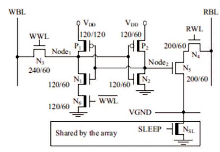
Hailong Jiao et al. Introduced a new asymmetrically ground-gated nine-transistor SRAM cell. The MTCMOS technique was used in their paper. The data stability is decreased as scale down CMOS technology node. Figure 1 shows that the data stability and technology are in proportional to each other, as in 90 nm technology, the data stability is higher and in 22 nm technology, the data stability is lower. There is relation between soft error rate and power supply (Vdd). Energetic cosmic rays or alpha-particles can induce soft error easily in sub threshold region compared to super threshold region because the critical charge (Qc) in subthreshold region is reduced with Vdd scaling in nanometer technology. Hazucha et al. (2003) reported that SER increases by 18% for each 10% reduction in Vdd (Jiao et al., 2016).
Figure 1. Read and Write Static Noise Margin on Different Technologies (Jiao et al., 2016)
Ground gated circuits are also presented in this paper. In conventional 6T SRAM cell for low power application, centralized High Threshold Voltage (HVT) sleep transistor is used. This sleep transistor disconnects the memory array from the ground during sleep mode. An 8T SRAM cell is described in (Upadhyay et al., 2015). As compared to conventional 6T SRAM cell, two extra transistors are added. By adding these extra transistors, read port is separated. The data stability of read operation is increased compared to the conventional 6T SRAM.
The structure of SRAM cell consists of nano-wire transistor. Simulations are done for static noise margin. The static noise margin evaluates on different operating voltages and threshold voltage. The performance benefits of undoped nanowire-transistor-based SRAM are measured in terms of the read stability for low voltage and low offleakage current operation (Tanaka et al., 2015).
Stability of the proposed SRAM has improved due to the reduction in swing voltage. Simulation results of power dissipation, access time, current leakage, stability, and power delay product of the proposed SRAM cell have been determined and compared with those of some other existing models of SRAM cell. Simulation has been done in 45 nm CMOS environment (Upadhyay et al., 2015; Predictive Technology Model (PTM)).
The structure of SRAM cells are having bitlines for read and write operation, but there is a drop in voltage during write operation. The tolerable limit of word-line voltage drop is known as Word Line Voltage Margin (WLVM). Their experimental measurement can be attained with minimal design modifications, while achieving good correlation with existing write ability metrics (Alorda et al., 2016).
The 12T SRAM bit cell is more robust in static and dynamic noise margin as compared to the conventional 6T SRAM cell, 8T SRAM bit cell, and 10T SRAM cell from the Monte- Carlo (MC) simulation results. The area overhead of the 12T SRAM cell is enhanced by 1.96 times and 1.74 times as compared to the 6T SRAM cell and 8T SRAM cells, respectively (Kim and Mazumder, 2017).
Two ground-gated memory circuits are presented in this paper. Multi-threshold CMOS (MTCMOS) is a variation of CMOS chip technology which has transistors with multiple threshold voltages (Vth) in order to optimize delay or power. The asymmetrical 9T SRAM cell provides larger read current and shorter read delay. The Half-select technique is used in 9T SRAM cell for higher (Jiao et al., 2016a).
Jiao et al. (2016b) proposed a new asymmetrically groundgated seven-transistor SRAM cell. This new cell is introduced for providing a low leakage current and high data stability in sleep mode. The 65 nm CMOS technology is used for simulation. In their paper, the 7T SRAM cell was compared with the previously works on 6T and 8T SRAM cells. A special write circuitry is used for write operation in this 7T SRAM cell. The ground-gated technology is used to break the connection between power supplies to ground in idle mode, so that leakage current can reduce in sleep mode. A sleep transistor is connected between sources of access transistor to ground under the ground-gated technology. This sleep transistor works on high threshold value and ensures that there is no connection between power supply Vdd to ground in sleep mode. For read operation, the output single-ended sense amplifier is connected at read port. In conventional 6T SRAM, the read and write operation performs on same bitline. So bitlines have to recharge at Vdd after every write operation repeatedly. Therefore 7T SRAM cell does not need to be recharged to Vdd after write operation because in this write, bitline is used only for write operation. Due to this difference, power consumption by memory array is higher in 6T SRAM cell compared to 7T SRAM cell. Leakage power can be reduced by using bit cell technique. This technique is affected by various parameters of SRAM cell (Shrivas and Akashe, 2012).
The same port is shared for read and write operation in SRAM cell. If read and write will be separated, then leakage power consumption and stability can be improved. The 9T SRAM cell has different port for read and write operation, so this cell has better stability and low power dissipation (Akashe et al., 2012). There are multi-threshold voltage devices and various circuit techniques for power reduction and performance improvement (Wang et al., 2015).
There is a technique for improving write operation of SRAM cell, i.e. write assist technique. In this technique two different type of voltages are applied on both bitlines. Negative voltage is applied on one bitline while boosted voltage is applied on another bitline. This technique is applied on 10T SRAM cell the and resultant is low leakage power with low supply voltage (Farkhani et al., 2015).
There is another problem, i.e. voltage swing between bitline and bitbar line at the output, which increases the power dissipation. To reduce this problem, two voltage sources should be connected. One voltage source can connect with bitline and another can connect with bitbar line (Upadhyay et al., 2015). The total power consumption of SRAM cell upto 5.43 μW can be reduced by lowering the power supply Vdd at 0.35 V (lower than the threshold voltage) (Wu et al., 2016).
The reason of power dissipation is voltage swing in write operations, as discussed above. The charge pump is used in SRAM cell to reduce power loss and it can store and reuse bitline charge. This charge recycling SRAM cell is also designed to improve read or write stability (Wang et al., 2016).
There are various techniques introduced to reduce leakage current. Mostly, process and circuit level techniques are used for reducing leakage current. The leakage current is reduced at process level by controlling the dimensions of SRAM cell. To reduce leakage currents, these techniques use relation between power supply and threshold voltage, as well as the concepts of stacking effect and body biasing (Butzen and Ribas, 2006).
MTCMOS stands for Multi Threshold CMOS. This technique is used for suppressing sub threshold leakage current. The sub threshold leakage current flows from power supply to ground in sleep mode. In this technique, different threshold values can be applied on different transistors in a single circuit. High threshold voltage transistors (header and/or footer) are connected from low threshold voltage transistors to power supply and/or ground connections.
There is a different power and ground gated circuits for improving sub threshold leakage current (Jiao and Kursun, 2010; Siebel et al., 2012).
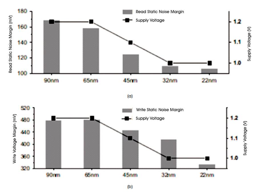
A tri-mode MTCMOS technique is used, where high threshold voltage NMOS and high threshold voltage PMOS are connected in parallel with each other. These circuits operate in three modes: sleep mode, park mode, and active mode. Two different ways for connecting header and footer is shown in Figures 2 and 3.
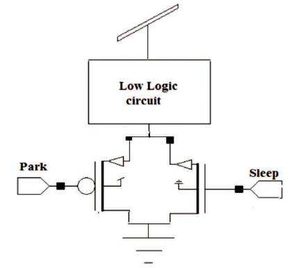
Figure 2. Power and Ground Gated Tri-mode MTCMOS (Footer) (Jiao and Kursun, 2010)
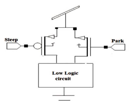
Figure 3. Power and Ground Gated Tri-mode MTCMOS (Header) (Jiao and Kursun, 2010)
3.2.1 Circuit Description of 6T, 7T, 8T, and 9T SRAM Cell
Conventional 6T SRAM cell are characterized on different cell ratio with three different threshold voltage levels: low, high, and dual. Figure 4 shows the conventional 6T SRAM cell with ground-gated technique. In this ground-gated technique, two transistors are connected (SLEEP and HOLD) between bistable circuitry and real ground line. In active mode, the SLEEP transistor is activated while the HOLD transistor is in OFF condition. In sleep mode, SLEEP transistor is in OFF condition while HOLD transistor is activated. There are two purposes for this technique, at first to minimize the leakage current in sleep mode and second is to maintain a sufficient voltage difference between Vdd and VGND (Jiao and Kursun, 2010). Here the authors have used traditional structure of 6T SRAM cell as shown in Figure 4 with different threshold configurations.
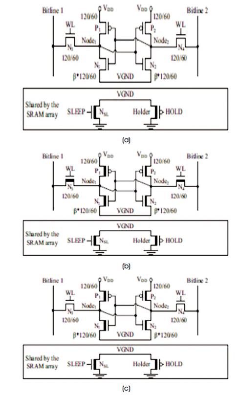
Figure 4. Conventional 6T SRAM Cell with Ground Gated Technique, (a) LVT 6T SRAM Cell, (b) HVT SRAM Cell, (c) DVT 6T SRAM Cell (Jiao et al., 2016)
The asymmetrical 7T SRAM circuit is illustrated in Figure 5 storing information in the cross coupled inverters. The read and write ports are separated from each other in this circuitry. The read port consists of access transistor N4 and a NMOS transistor N5 . The ground-gated technique is used in this circuit to suppress the leakage current (Jiao et al., 2016).
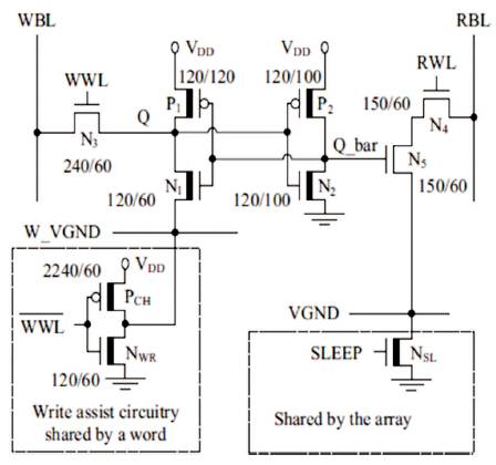
Figure 5. The Asymmetrical Ground-gated 7T SRAM Cell (Jiao et al., 2016).
The asymmetrically ground-gated 8T SRAM circuit is shown in Figure 6. This cell consists of two extra transistors compared to 6T SRAM cell. The MTCMOS technique is used for suppressing the leakage current. The sleep transistor is connected between sources of read transistor to ground in sleep mode. A new transistor is added in this circuitry to increase the write ability. The target is to separate read port with write port (Jiao et al., 2016).
The circuit is shown in Figure 7. In this cell, three transistors are extra added with conventional 6T SRAM cell. Compared to 8T SRAM cell, one extra PMOS transistor is added between power supplies to PMOS transistor of first inverter.
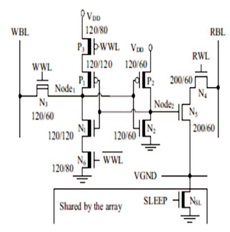
Figure 7. The Asymmetrical 9T SRAM Cell (Jiao et al., 2016).
In this section, three parameters, viz., stability, delay, and power dissipation are compared to each other for different SRAM cells. The 70 nm technology is used for simulation of Predictive Technology Model (PTM).
The read, write, and hold SNMs are compared in this section and it is shown in Table1. Stability directly relates to SNM and SNM is defined as maximum DC noise voltage that can be tolerated by an SRAM cell without losing the data during read and sleep operation.
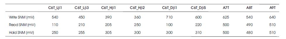
Table 1. Comparison of SRAM Cells for Stability (Jiao et al., 2016)
(a) Write Mode: In write mode, the DVT conventional ground-gated 6T memory cell with β=1(C6T_Dβ1) has the highest SNM among the other configurations that are presented in this section. Alternatively, the HVT conventional ground-gated 6T SRAM with β=2 (C6T_Hβ2) has the minimum SNM as shown in Table 1. The write SNM of conventional 6T SRAM cell (C6T_Dβ1) is enhanced by 13.6%, 31.48%, 10.93%, respectively, as compared to the asymmetrical 7T SRAM cell, asymmetrical 8T SRAM cell, and asymmetrical 9T SRAM cell.
(b) Read Mode: In read mode, the asymmetrical groundgated 9T memory cell has the highest SNM among the other configurations that are presented in this section. Alternatively, the DVT conventional ground-gated 6T SRAM with β=1 (C6T_Dβ1) has the minimum SNM as shown in Table 1. The read SNM of asymmetrical 9T SRAM cell is enhanced by 410%, 2%, 4.08%, respectively, as compared to the conventional 6T SRAM cell (C6T_Dβ1), asymmetrical 7T SRAM cell and asymmetrical 8T SRAM cell. The asymmetrical 9T SRAM cell has better stability compared to other SRAM cell for read mode of operation. The reason behind is that the structure of asymmetrical 8T SRAM cell. It has different read port from the write port, so the bitlines can precharged from 0 to Vdd without any disturbance.
(c) Hold Mode: In hold mode, the asymmetrical groundgated 9T memory cell has the highest SNM among the other configurations that are presented in this section. Alternatively, the LVT conventional ground-gated 6T SRAM with β=1 (C6T_Lβ1) has the minimum SNM as shown in Table 1. The hold SNM of asymmetrical 9T SRAM cell is enhanced by 104%, 2%, 6.25%, respectively, as compared to the conventional 6T SRAM cell (C6T_Lβ2), asymmetrical 7T SRAM cell, and asymmetrical 8T SRAM cell. In this operation, asymmetrical 9T SRAM cell shows better stability compared to others. In hold mode, data is stored in cross coupled inverters. To maintain the stability of data, two extra NMOS transistors are connected between cross coupled inverters to power supply and ground of asymmetrical 9T SRAM cell. Due to these extra transistors, the stability of asymmetrical 9T SRAM cell is higher compared to other SRAM cells.
(a) Write Mode: In write mode, the DVT conventional ground-gated 6T memory cell with β=1(C6T_Dβ1) has the minimum delay among the other configurations that are presented in this section. Alternatively, the asymmetrical ground-gated 7T has the maximum delay as shown in Table 2.
Read Mode: In read mode, the asymmetrical groundgated 7T memory cell has the minimum delay among the other configurations that are presented in this section. Alternatively, the HVT conventional ground-gated 6T SRAM with β=1 (C6T_Hβ1) has the maximum delay as shown in Table 2. The read delay of asymmetrical 7T SRAM cell is suppressed by 44.44%, 1.96%, 1.31%, respectively, as compared to the conventional 6T SRAM cell (C6T_Hβ1), asymmetrical 8T SRAM cell, and asymmetrical 9T SRAM cell. The read port is different from the write port in the structure of 7T SRAM cell and the size of read port transistors are less compared to other transistors. So the speed of operation is higher for 7T SRAM as compared to other SRAM cells.
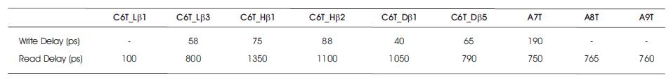
Table 2. Comparison of SRAM Cells for Access Delay (Jiao et al., 2016)
(a) Write Mode: In write mode, the asymmetrical groundgated 8T has the minimum power consumption among the other configurations presented in this section. Alternatively, the HVT conventional ground-gated 6T SRAM with β=5 (C6T_Dβ5) has the maximum power consumption as shown in Table 3. The write power consumption of asymmetrical 8T SRAM cell is suppressed by 40%, 2.3%, 4.54%, respectively, as compared to the conventional 6T SRAM cell (C6T_Lβ3), asymmetrical 7T SRAM cell, and asymmetrical 9T SRAM cell. The asymmetrical 8T SRAM cell has write assist transistor to prevent for flowing of leakage current.
(b) Read Mode: In read mode, the conventional groundgated 6T SRAM with β=1 (C6T_Hβ1) memory cell has the minimum power consumption among the other configurations presented in this section. Alternatively, the asymmetrical ground-gated 8T has the maximum power consumption as shown in Table 3. The read power consumption of conventional 6T SRAM cell (C6T_Hβ1) is suppressed by 28.37%, 37.91%, 33.04%, respectively, as compared to the asymmetrical 7T SRAM cell, asymmetrical 8T SRAM cell, and asymmetrical 9T SRAM cell. The conventional 6T SRAM cell with high threshold value of inverters prevents leakage current in read mode.
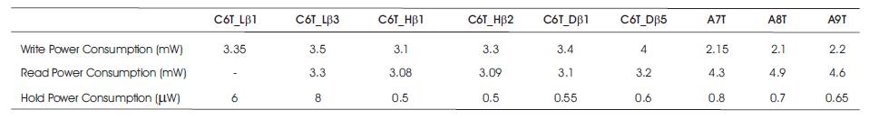
Table 3. Comparison of SRAM Cells for Power Consumption (Jiao et al., 2016)
(c) Hold Mode: In hold mode, the HVT conventional ground-gated 6T SRAM with β=1 (C6T_Hβ1) memory cell has the power consumption among the other configuration that are presented in this section. Alternatively, the DVT conventional ground-gated 6T SRAM with β=3 (C6T_Lβ3) has the maximum power consumption as shown in Table 3. The hold power consumption of conventional 6T SRAM cell (C6T_Hβ1) is suppressed by 37.5%, 28.5%, 23.07%, respectively, as compared to the asymmetrical 7T SRAM cell, asymmetrical 8T SRAM cell, and asymmetrical 9T SRAM cell. In HVT configuration of 6T SRAM cell, all the transistors are on high threshold value with sleep transistor and this sleep transistor prevents leakage current in hold mode as discussed in MTCMOS tri mode operation.
The various performance parameters, such as noise margin, delay, leakage power, and access time for SRAM cell architectures are characterized in this paper. Comparison of 6T, 7T, 8T, and 9T SRAM cell with different beta ratio are considered and their simulations have been analyzed. From the simulation results, it is concluded that the write SNM of conventional 6T SRAM cell (C6T_Dβ1) is leading as compared with the asymmetrical 7T SRAM cell, asymmetrical 8T SRAM cell, and asymmetrical 9T SRAM cell.
The read SNM of asymmetrical 9T SRAM cell is better as compared to the conventional 6T SRAM cell (C6T_Dβ1), asymmetrical 7T SRAM cell, and asymmetrical 8T SRAM cell. Hence, asymmetrical 9T SRAM cell has better stability compared to other SRAM cell for read mode of operation. The asymmetrical 7T has highest read delay and 6T with high threshold voltage at maximum delay during write operation. The HVT conventional ground-gated 6T SRAM with β=1 has highest delay due to high threshold voltage transistors. The write power consumption of conventional 6T SRAM cell (C6T_Hβ5) read power consumption for asymmetrical 7T and hold power consumption of conventional 6T SRAM cell (C6T_Lβ3) is largest. From this paper, it is concluded that there is a trade-off between various SRAM cell architecture for various performance parameters, highly stably SRAM cell has large delay, and for high speed SRAM memory cell is power hungry. Hence for specification or application, designer can choose best memory cell architecture and by selecting proper W/L ratio of SRAM cell transistors better results can be obtained.s