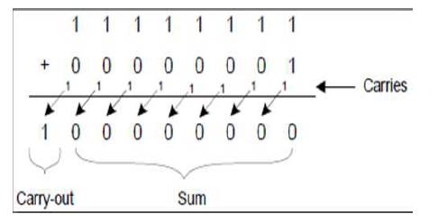
Figure 1. Binary Adder
Binary Addition is one of the most important arithmetic operations that a processor can execute. Such ALU process requires to be operated with high speed without degrading the performance of the circuit. Since VLSI mainly focuses in area, delay, and power consumption, a good VLSI circuit can maintain tradeoff between these parameters. In this paper, Parallel Self Timed Adder (PASTA) is presented, which is capable of performing multipath binary addition. This parallel operation do not generate carry chain propagations, thereby speedup the circuitry. One advantage of parallel adder is it maintains the tradeoff between Fan-in and Fan-out by incorporating suitable transistors in parallel. The design is implemented in Xilinx ISE14.2 synthesis tool with Virtex-5 FPGA as the target hardware equipment. For backend analysis, the XOR gate and multiplexers are designed by using extended Dual Mode Logic Technique and layouts are designed in Microwind3.1 at 32 nm CMOS Technology. The simulation and synthesis results reveal the fact that the parallel self timed adder has the potential to run faster when compared to existing asynchronous adder.
To humans, decimal numbers are simple to grasp and implement for performing arithmetic operations. However, in digital systems, like a microchip, DSP (Digital Signal Processor), or ASIC (Application-Specific Integrated Circuit), binary numbers are much more sensible for a given computation. This happens as a result of the binary values that are optimally economical at representing several values. Binary adders are one among the foremost essential logic components inside a digital system. In addition, binary adders are also useful in units apart from Arithmetic Logic Units (ALU), like multipliers, dividers, and memor y addressing. Therefore, binar y addition is important that any improvement may end up during a performance boost for any DSP system and, hence facilitate in improving the performance of the whole system.
The major drawback for binary addition is the carry chain. Figure 1 demonstrates an example of an 8- bit binary add operation and the way carry chain is affected. This instance shows that the worst case occurs when the carry travels the longest possible path, from the Least Significant Bit (LSB) to the Most Significant Bit (MSB). As the width of the input operand increases, the length of the carry chain increases. In order to enhance the performance of carry-propagate adders, it is attainable to accelerate the carry chain, however not eliminate it. Consequently, most digital designers typically resort to assembling quicker adders, as a result of this they have a tendency to line the important path for many computations.
Figure 1. Binary Adder
The binary adder is the crucial component in most digital circuit styles together with Digital Signal Processors (DSP) and microchip information path units. Such, intensive analysis continues to be centered on rising the ability delay performance of the adder. In VLSI implementations, parallel Self Timed Adders are known to have the best performance approaches.
The power advantage is especially important with the growing popularity of mobile and portable electronics, which make extensive use of DSP functions. However, because of the structure of the configurable logic and routing resources in FPGAs, parallel-prefix adders will have a different performance than VLSI implementations. In particular, most modern FPGAs employ a fast-carry chain which optimizes the carry path for the simple Ripple Carry Adder (RCA). In this paper, the practical issues involved in designing and implementing tree-based adders on FPGAs are described.
Most of the adders’ area unit are designed for synchronous circuits even there is an interest in clock-less asynchronous processors (Geer, 2005). Asynchronous circuits does not need any quantization time and that they will capable of holding sensible logic styles. Usually asynchronous adders area unit supported null convention logic (Sparsø and Furber, 2001) or pipelined operation. In asynchronous systems, a sub-system will simply get replaced by another system with identical practicality, however with totally different performance, however this cannot be an easy task, just in case of a synchronous system because the c l o c k amo u n t ma y n e e d t o b e r e c omp u t e d. Asynchronous system stage involves acknowledgment (signal exchange) sign protocol which is shown in Figure 2. However, strong asynchronous systems provide the request data at intervals, the info wires and area unit are typically considered as self-timed systems.
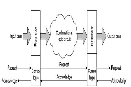
Figure 2. An Asynchronous System Stage
This paper explains about asynchronous parallel self timed adder (Choudhury et al., 2008). The design of PASTA consists of half-adders and multiplexers with minimum routing paths. The design is capable of working in parallel manner for independent carry chain blocks. The hardware unit of PASTA consists of an XOR gate through which feedback mechanism is developed for asynchronous sequential adder (Rahman and Kleeman, 2013). In most VLSI architectures, XOR gate is most widely used as it contains less clock control signals and it is readily available as an ASIC product. In this paper, XOR gate and multiplexers are designed by using DML technique. Cyclic circuits can be more efficient than the acyclic counterparts, which are referred in Riedel (2004) and Tinder (2009). To stabilize the outputs, pipelining can be used as the input which is discussed by Liu et al. (1994) and Tewksbury and Lee (1994).
The half adder adds two one-bit binary numbers A and B, which is shown in Figure 3. It has two outputs, S and C (the value theoretically are carried on to the next addition); the final sum is 2C + S. The half adder circuit shown in Figure 3 consists of an XOR gate to generate result of sum noted as S, the AND gate to generate carry results noted as C. If two half adders are combined, then a full adder circuit is designed and an extra OR gate is used at the output stage to generate carry outputs.
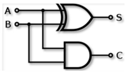
Figure 3. Half Adder
One-bit full adder is shown in Figure 4. It adds three one-bit numbers, often written as A, B, and C ; A and B are the in operands, and C is a bit carried in from the next less in significant stage. The full-adder is usually a component in a cascade of adders, which adds 8, 16, 32, etc., binary numbers. The circuit produces a two-bit output sum typically represented by the signals C and S, where,
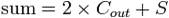
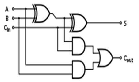
Figure 4. Full Adder
The Carry Look Ahead Logic is shown in Figure 5. It can verify whether or not that bit combined will generate a carry or propagate a carry. This permits the circuit to "pre-process" he 2 numbers being further to see the carry prior time. Then, once the particular addition is performed, there is no delay from expecting the ripple carr y result. The disadvantage of the CLA adders is that the carry expressions become quite complicated for quite four bits.
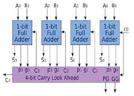
Figure 5. Carry Look Ahead Adder
The general design of the PASTA is shown in Figure 6. The selection input for two-input multiplexers correspond to the required handshake signal and can be one zero to one transition denoted by SEL. It will choose the particular operands throughout SEL=0 and will switch to feedback or carry methods for future iterations if SEL=1. The feedback path from the HAs permits the multiple iterations to continue till completion, once all carry signals can assume zero values.
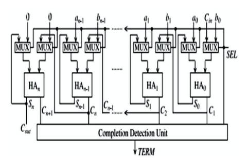
Figure 6. Parallel Self Timed Adder (PASTA)
The Architecture of Parallel Adder consists of initial phase and iterative phase, which is shown in Figure 7. During initial phase, the circuit works as a combinational half adder and just similar to fundamental operating mode of adder. One advantage of using Half Adder instead of full adder is the state (11) cannot appear. During the iterative phase (SEL=1), the feedback through multiplier is activated. The proposed design cannot be considered as a fundamental node as the input-output will go through several transitions before generating the final output. The design is capable of working in parallel manner for independent carry chain blocks.
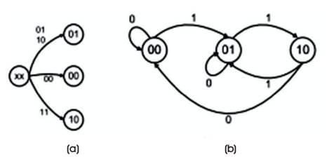
Figure 7. State Diagram for PASTA (a) Initial Phase, (b) Iterative Phase
In the design of parallel adder multiplexer, half adder circuits are most widely used. The operation of half adder and the description as in Figure 1. The multiplexer is shown in Figure 8. Multiplexer acts as both combinational and sequential circuit and particularly used for generating the results based on selection. In this paper, the multiplexer is modeled by using Dual Mode Logic (DML) technique. To reduce the hardware components and the count of transistors the design is modeled using Transmission gates.
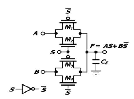
Figure 8. Transmission Gate Multiplexer
DML gates are existing with two possible topologies, 1) Type A and 2) Type B, as shown in Figure 9. The concept of DML technique is explained by taking CMOS inverter as shown in Figure 10. In this, DML acts as keepers and maintain the tradeoff between pull up and pull down transistors during switching and thus increases the performance of the circuit.
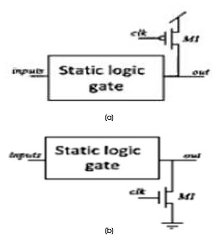
Figure 9. DML Topology
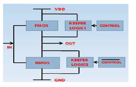
Figure 10. DML Operation
The front end analysis of the proposed design is modeled by using Xilinx14.2 by choosing Verilog as the Hardware descriptive language and the design is modeled for Virtex5 FPGA. The top module of 64 bit PASTA is shown in Figure 11 and the technology schematic is shown in Figure 12.
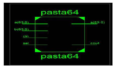
Figure 11. PASTA Top Module
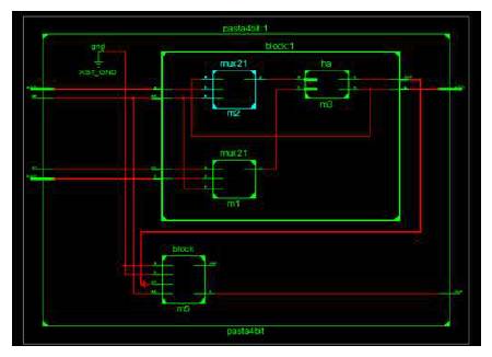
Figure 12. Technology Schematic
The design summary is reported in Figure 13 and it is related to the target FPGA which gives the data on the number of slice registers and Look up tables are required for the design and the delay associated with the circuit. Since FPGA is field programmable, if any error occurs in the design, those can be easily rectified. The synthesis report is shown in Figure 14 with a delay factor of 42.576 ns.
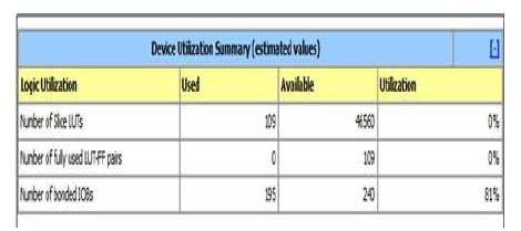
Figure 13. Design Summary
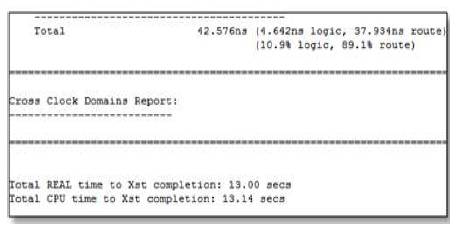
Figure 14. Synthesis Report
The multiplexer is designed by using lambda based design rules by following Dual Mode Technique and Microwind3.1 as the backend tool and it is presented in Figure 15.
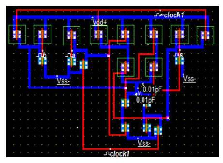
Figure 15. Multiplexer with DML Technique
In this paper, a parallel self timed adder has been described for processing ALU operations. The design is modeled with referencing simplified circuits with no carry propagation delays. The PASTA architecture is operated with initial and iterative phase and the design is simplified.
This work eliminates the need of extra hardware components to control, thereby reduces the transistors count. With the transmission gate logic, the hardware components are reduced, thereby area can be minimized and power required to dive the hardware components is reduced. The design is modeled for 64 bit parallel adder operations and in future the design is modeled up to 128 bit without disturbing the hardware architecture. Microwind3.1 backend tool is used in this article to design the multiplexer. The experimental results shown in Table 1 proves the effectiveness of the proposed design with good performance for ALU processing applications.
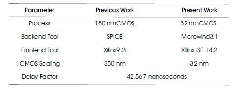
Table 1. Comparison of Results