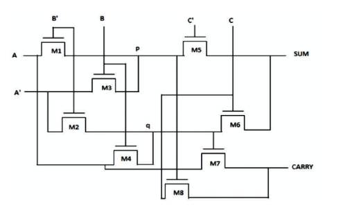
Figure 1. Proposed Full Adder
Power dissipation is an important parameter in VLSI circuits. Previously it was ignored due to low device density and low operating frequency. Due to the challenging issues on high packing density, high operating frequency and increase in portable consumer electronics, high heat dissipation occurs which damages the performance. The previous method using 1 bit full adder was not sufficient in handling high performance circuit. The proposed method reduces the power dissipation of a device and at the same time maintains an adequate throughput. For any processor, Full Adder is an important block for all processing and execution of mathematical models. By using Pass Transistor Logic (PTL) redundant transistors can be eliminated, which in turn increases the speed and reduces the heat. The proposed method of including NMOS based PTL increases the performance of 1 bit and 8 bit full adder with more transistors in low area for an efficient power handling method. The results of the proposed work is compared with XOR existing method. The proposed full adder is efficient in terms of power frequency and area.
Now-a-days, the personal computing devices and wireless c ommu n i c a t i o n s y s t ems d ema n d h i g h s p e e d computation with low power consumption (Karimi et al., 2018; Karimi and Rezai, 2017; Balali et al., 2017). There are many reasons for demanding low power consumption. The main reason is to increase the battery life time of portable devices. Another drawback in battery technology is increasing battery size due to higher energy capacity. The second reason is the reliability of the system. If the power dissipation is more, then heat sink or cooling device should be provided (Weste and Eshraghian, 1994). Otherwise electrical parameter shift will occur. Indirectly packaging cost of the device is also increasing. So to overcome all these issues, designing a device which will consume less power is vital. To do a high speed computation, an efficient arithmetic logic unit is needed. Full adder is an important block in ALU. So in this paper, the authors propose a 1-bit and 8-bit Full Adder, which will consume low power using PTL logic.
Various Logic styles have been proposed for designing Full Adder. Static CMOS full adder with pull up and pull down transistor has been proposed which provide full swing output. But speed of the system is degraded due to high input capacitance. In this paper, complementary pass transistor logic style has been proposed which is having full swing output, high speed, and high power dissipation. (Zimmermann and Fichtner, 1997). Full adder is designed with transmission function which is having low power dissipation, but low driving capability (Zhuang and Wu 1992). A new full adder is proposed based on multiplexer which impacts with threshold problem on its output node (Jiang et al., 2004). Formal Design Procedure is developed using K-map and Pass network theorem for designing Full adder with 6 transistor of XOR-XNOR cell, which does not have threshold voltage problem. But some more design effort is needed for sizing of the device (Radhakrishnan, 2001). In another paper, the power consumption was reduced by reducing the supply voltage below threshold voltage (Alioto and Palumbo, 2002; Dokania and Islam, 2015; Guduri and Islam, 2015; Dokania et al., 2017). Using carbon nanotube field effect transistor device, power consumption was reduced in full adder (Mehrabani and Eshghi, 2016).
The objective of the pass transistor logic in defining the speed and power consumption includes the transistor size and reliability. The proposed method reduces the number of transistors, therein maintaining the same performance by using a combination of XOR and XNOR. The flexibility in the transistor size is maintained by the Pass transistor logic, thereby achieving the power reduction. More number of such logic can be fabricated for multiple chip functions further reducing the complexity for high functionalities.
Pass Transistor Logic is used in Integrated Circuits to reduce the number of transistors in the circuit by eliminating redundant transistor. It uses few transistors, which will have more speed and low power consumption. So in this proposed work full adder is designed with pass transistor Logic.
Full Adder will have 2 inputs A, B, one carry in C and 2 outputs Sum and Carry out. The Logic equation of full adder is as follows,
The basic module of full adder circuit is XOR and XNOR gate. By using simple OR, NOT, and AND gates, the authors have designed these modules. The main factor to consider is the number of transistors used. If it increases, then it will affect the power dissipation and delay. Considering all these factors, a circuit has been designed. The first transistor M1 is generating the output AB' while M3 is generating output A'B. The two outputs together generates (A Å B) at point P. The outputs of M2 and M4 are A'B' and AB, respectively. They produce AB at point Q. The logic at the outputs of M5 and M6 are (A Å B) C' and (AB)C. They are generating the sum output in the following manner.
Similarly the output logic of M7 and M8 generate the carry value.
The proposed full adder circuit is shown in the Figure 1 with 8 transistors. Table 1 will explain the logic values at the output levels of transistor for different input combinations of the circuit.
Figure 1. Proposed Full Adder
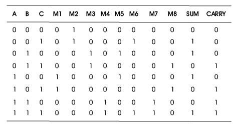
Table 1. Truth Table for Proposed Full Adder
For 8-bit full adder, ripple carry adder is used. Ripple carry adder is created using cascading multiple adders. Each full adder input carry is a carry out of previous adder. In 8-bit full adder, to add two bytes of data together, the adder looking after the rightmost column of binary digits would indeed need to be nothing more than a half adder. However, all the adders to the left of that need to able to accept three inputs- two digit from their column and any carry from next column to the right.
Figure 2 explains the circuit connection for 8-bit full adder. Here 8 numbers of 1-bit full adder are connected in cascade form to make 1-bit full adder into 8-bit full adder.
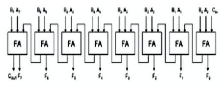
Figure 2. 8-bit Full Adder
Truth table will give the logical output for all possible outputs. The truth table for 8-bit full adder using ripple carry adder is given in Table 2.
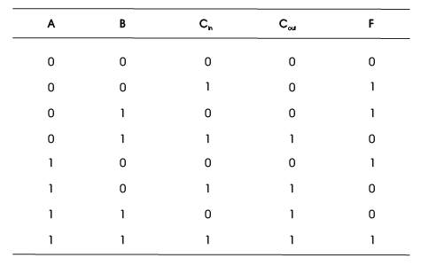
Table 2. Truth Table for Ripple Carry Adder
All the simulations are performed on microwind 3.5 and DSCH 3.5 using 65 nm. Microwind is an electronic automation tool for designing integrated circuits in physical level. Before designing the circuit, architecture is validated at the logic level using DSCH module in Microwind. DSCH module is used to evaluate the power consumption.
The main concept of the work is to face all challenges in designing 1-bit and 8-bit full adder circuit using NMOS method based on Pass transistor logic. This work develops a NMOS design methodology for full adder circuit combining gates of different logic to same circuit in an effort to obtain improved performance compared to XOR method. Layout design explains the placement of components in integrated circuit during fabrications. The Layout of 1-bit full adder using NMOS is given in Figure 3.
The simulation diagram is very important to verify their logic. From the simulation diagram, the function of the circuit can be checked. In Figure 4, the truth table of full adder is verified. The simulation results of 1-bit full adder using NMOS is shown in Figure 4.
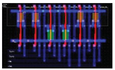
Figure 3. Layout Diagram of 1-bit Full Adder
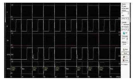
Figure 4. Simulation Diagram of 1-bit Full Adder
In Figure 5, the layout of 8-bit full adder using NMOS is described. It will give the placement of components and routing, i.e interconnection to the components.
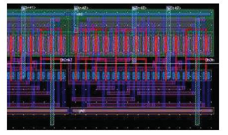
Figure 5. Layout Diagram of 8-bit Full Adder
The simulation results of 8-bit full adder using NMOS is shown in Figure 6. Here each input has 8-bit.
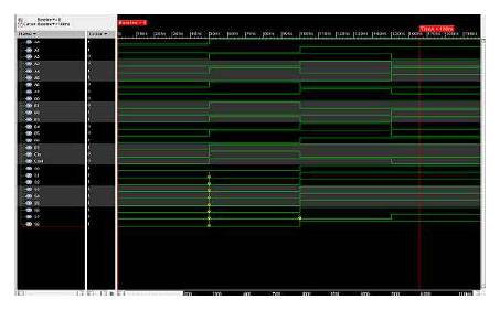
Figure 6. Simulation Diagram of 8-bit Full Adder
Power consumption can be calculated using DSCH module in Microwind Software.
In Figure 7 power consumption of the proposed method calculated is shown. Table 3 describes the comparison between proposed 1-bit full adder method and XOR method in terms of area, power, and frequency. In this proposed method, the number of transistors used are reduced. Because of that the area also gets reduced. The main aim of reducing power consumption is also achieved.
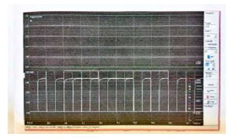
Figure 7. Simulation Diagram of 1-bit Full Adder
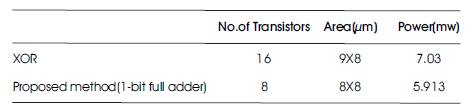
Table 3. Comparison of Full Adder Designs
Table 4 will give the comparison between 1-bit full adder and 8-bit full adder in terms of number of transistors used in power consumption. Here in 8-bit full adder, the number of transistors and power consumption are increased. But on comparing with XOR method, this output is reasonable.
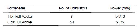
Table 4. Comparison of 1-bit and 8-bit Full Adder
The proposed method with the combination of XOR and XNOR using Pass Transistor logic shows that proposed full adder circuits consumes less power and area as compared to other full adder circuits. The simulation and layout diagrams generated gives a clear fact of reduced power performance even after reducing the number of transistors.
Further analysis is performed for observing the area after reducing number of transistors, offered a very good layout structure with maximum yield at the time of fabrication with the help of microwind software. The performance degradation at higher load capacitance is a major concern of this method and needs to be eliminated in future with the help of other advanced technologies.