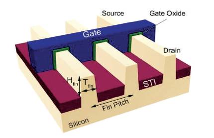
Figure 1. 3D Cross Section View of FinFET
Due to scaling of conventional MOS transistors, leakage currents are increasing which leads to increase in power dissipation. Increase in power dissipation puts limit on scaling. To overcome the power dissipation problem, conventional MOS transistors are replaced with FinFETs. FinFETs have low leakage currents which reduce power dissipation. In this paper the focus is on the implementation of different full adder circuits using FinFETs. Comparisons are made between CMOS and FinFET implementation of Hybrid Full Adder, 14 Transistor Full Adder, GDI based Full Adder, and 10 transistor Full Adder using 32 nm and 45 nm technology models. FinFET implementation achieves low power and high speed compared to CMOS implementation.
Demand for compact processors with high speed and low power consumption is increasing day-by-day. The Arithmetic Logic Unit (ALU) plays a major role in Central Processing Unit.
Major arithmetic operation performed by ALU is addition. Adders play major role in Signal processing, Image processing and VLSI Applications. Demand for high speed and low power adders has led many researchers to focus on the design of efficient adders [22]. Scaling is one of the methods to achieve reduction in delay and power consumption. Due to scaling, the short channel effects like sub-threshold current, leakage current, and hot electron effects will increase, resulting in increase in power dissipation. These effects put a limit on scaling of conventional MOS transistors [24]. FinFET devices are the solution for narrow scaling. FinFET devices provide low power, high speed compared to conventional MOS transistors [13].
Full adder circuit designs are classified into two types based on the output. One type is with full swing output and the other without full swing output. Complementary CMOS (CCMOS Complementary Pass Transistor Logic (CPL), Transmission Gate (TGA), Transmission Function (TFA), Hybrid, 14 Transistor (14T), and 16 Transistor (16T) based full adder designs belongs to first type, which produces full swing output [10], [11], [23], [26], [27]. 10 Transistor (10T), 9 Transistor (9T), and 8 Transistor (8T) based full adder designs belong to second type, which does not produce full swing outputs [4], [16], [25], [28], [31].
The advantage of C-CMOS full adder designs[12, 33, 34], is its flexibility in voltage scaling and transistor sizing to achieve reliable operation. CPL designs which use 32 transistors [1], [5], [6], [30] contribute to low power consumption. The disadvantage is it suffers from static power dissipation due to low swing at the outputs of inverters. Double pass-transistor logic [20] and swing restored pass- transistor logic [4], [5], [20], [21] are of CPL type designs. The main disadvantage of Transmission gate logic circuit [7], [30], [34] is it requires more number of transistors to implement the same circuit. The advantage of transmission function full adder (TFA) [34], [35] is its high speed and less power dissipation compared to the conventional CMOS adders.
A full swing, low power and high speed full adders are proposed [8] by using GDI logic and Hybrid CMOS logic styles. Full adder proposed by [15] achieves high performance with reduced power delay product at low operating voltages. Low energy full adder design proposed in [29] is suitable for high speed VLSI circuit applications with less number of transistors.
From the literature survey it is evident that many researchers are working on different adder circuits to reduce the power dissipation and also to improve the operating speed.
The paper is organized as, section 1 presents the objective of the paper, section 2 provides discussion about FinFET technology, section 3 explains the Full Adder designs, section 4 describes the implementation of proposed adders, and section 5 contains simulation results and comparisons. Finally the paper is concluded.
The objective of this paper is to implement Full Adder circuits using FinFET devices for low power consumption and less delay. Different adders like Hybrid Full Adder, 14 Transistor Full Adder, GDI Based Full Adder, and 10 transistor full adder circuits are implemented using FinFET 45 nm and 32 nm technology models. Predictive Technology Model (PTM) is used to simulate the designs using HSPICE. Performance metrics like delay, average power dissipation, and PDP are compared with CMOS full adder designs as well as FinFET based full adder designs.
The performance of conventional MOS devices decays with scaling due to short channel effects. FinFETs are the replacement of MOSFETs because of its low power dissipation, high performance, and low operating voltages. FinFET devices are made in a tall and narrow silicon island called “finger”, “leg”, or “fin”. The gate of FinFET device is wrapped around all sides of the fin. This works as the channel of the transistor. Figure 1 shows the cross section of FinFET device.
Figure 1. 3D Cross Section View of FinFET
FinFETs are evolved from the concept of Multi Gate MOSFETs. FinFET consists of source, drain, and gate terminals. In Dual Gate (DG) FETs, there are two gates, Front Gate and Back Gate. The minimum feature size in Multi Gate FETs is the Fin width not the gate length. For DG FinFET, the effective channel width is given by,
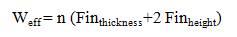
where n is the number of Fins.
Fin height and effective Fin width decides the current in the FinFET. The short channel effects are minimized by the gate electrode control in all directions.
The basic arithmetic operation in digital circuits is addition. Addition plays a major role in ALU. Full adder performs addition on three inputs (A, B, and Cin) and produces two outputs (Sum, Cout).
The truth table of Full Adder is given in Table 1.
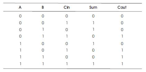
Table 1. Truth Table of Full Adder
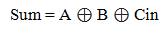
The Boolean expressions for Sum and Carry are generated by minimizing the truth table and the respective equations are given below.
Different full adder designs are proposed with tradeoff in power and speed. Hybrid Full Adder, 14 Transistor Full Adder (14T), Gate Diffusion Input Full Adder (GDI), and 10 Transistor Full Adder (10T) designs are simulated to observe the power consumption and delay.
Hybrid full adder consists of three modules. Modules 1 and 2 consists of XNOR modules to generate Sum, module 3 to generate Cout as proposed in [3]. The modules are designed such that the Full Adder is optimized in terms of power, speed, and area. The XNOR module is responsible for power consumption in Full Adder design. Module 1 consists of modified XNOR with less power consumption. Level restoring transistors Mp3, Mn3 guarantees full swing of output logic levels. Different XOR/XNOR modules are reported in [7], [9], [32]. The output Cout is implemented using transistors Mp7, Mn7, Mp8, and Mn8. Hybrid Full Adder circuit diagram is given in Figure 2.
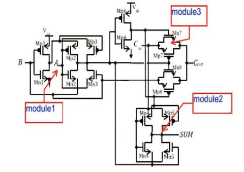
Figure 2. Circuit Diagram of Conventional MOS Hybrid FA
The 14T full adder uses 14 transistors to implement Sum and Cout[2]. It uses new XOR gate to produce half sum. Sum and Cout are generated by using new XOR gate and transmission gate [33]. The circuit diagram is shown in Figure 3.
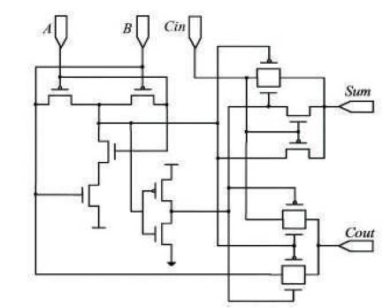
Figure 3. 14T Full Adder Circuit Diagram using Conventional MOS
The efficient way of implementing logic circuits is using Gate Diffusion Input logic proposed by [35]. GDI technique reduces power dissipation, area, and delay. The circuit diagram of GDI is shown in Figure 4 [17].
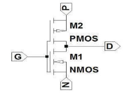
Figure 4. GDI Circuit Diagram
GDI consists of NMOS and PMOS transistors with common gate input, P input to source of PMOS, and N input to source of NMOS. The advantage of GDI technique is, it consumes less silicon area compared to other methods as it consists of less number of transistors, as the area is less the node capacitance is also less[18].
The logic circuit diagram of GDI Full Adder [19] is shown in Figure 5. The Full Adder consists of 2 XOR gates and 2 by 1 nd Multiplexer. Sum is produced at the output of 2 XOR gate and Cout is generated at the output of multiplexer
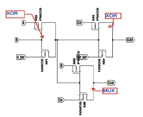
Figure 5. Circuit Diagram of GDI Full Adder
Static Energy Recovery Full adder (SERF) design proposed by [14] uses 10 number of transistors, which does not require inverted inputs. 10T FA consists of two 4-transistor XNOR circuits and one 2-to-1 multiplexer. The circuit diagram of 10T full adder is shown in Figure 6.
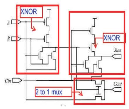
Figure 6. Circuit Diagram of 10T FA
Hybrid Full Adder, 14T FA, GDI FA, and 10T FA are implemented using 32 nm CMOS predictive technology model. The parameters used to simulate the circuits are given in Table 2.
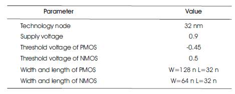
Table 2. 32 nm CMOS Technology Model Parameters
Figure 7 shows the simulation waveforms of CMOS Full Adder circuit.
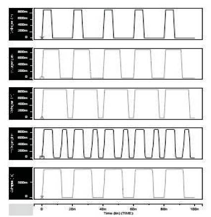
Figure 7. Simulation Waveforms of CMOS Full Adder
The simulation results and analysis of conventional MOS transistor Hybrid Full adder, 14T FA, GDI FA and 10T FA are given in Table 3.
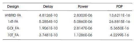
Table 3. Simulation Results of Conventional MOS Transistor based FAs
Hybrid Full adder, 14T FA, GDI FA, and 10T FA are implemented using FinFETs. The circuits are simulated using HSPICE with predictive technology models of 45 nm and 32 nm FinFET models
The technology parameters for 45 nm and 32 nm FinFET are given in Table 4.
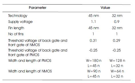
Table 4. FinFET 45 nm, 32 nm Technology Model Parameters
Figure 8 shows the simulation waveforms of FinFET full adder circuit. The simulation results and analysis of FinFET based Hybrid Full adder, 14T FA, GDI FA, and 10T FA are given in Table 5.
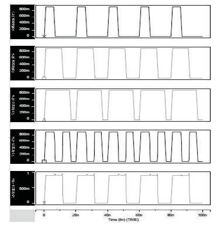
Figure 8. Simulation Waveforms of FinFET Full Adder
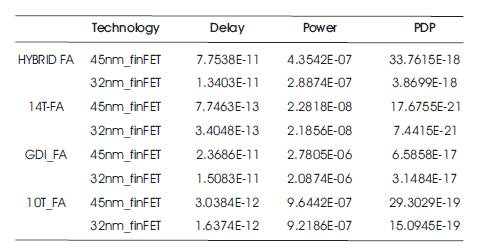
Table 5. Simulation Results of FinFET based Full Adders
The proposed full adders are designed using DG FinFETs. The proposed designs are simulated using HSPICE tool and compared with the CMOS designs. Comparison of simulation results of CMOS based full adders and FinFET based full adders are presented in Table 6 for the performance metrics delay, average power dissipation and PDP. Simulation results show that the FinFET full adders achieve high speed, low power dissipation than the conventional MOS based designs.
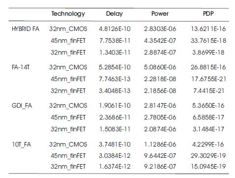
Table 6. Comparison of Simulation Results of CMOS based and FinFET based Full Adders
The delay comparison of implemented CMOS full adders is presented in Figure 9. The delay of GDI based full adder is less compared to other full adder circuits.
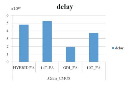
Figure 9. Delay of CMOS Full Adder Circuits
In Figure 10, comparison of the average power dissipation of different FA circuits is presented. It is evident that the power dissipation of 10 transistor full adder circuit is less compared to other full adder circuits.
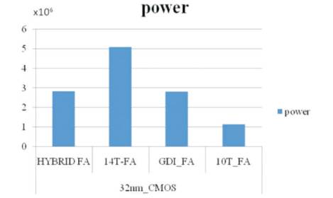
Figure 10. Average Power Dissipation of CMOS Full Adder Circuits
In Figure 11, the comparison of PDP for different FA circuits is given. PDP is the product of power and delay. The PDP of 10 Transistor based full adder circuit has low value compared to other designs.
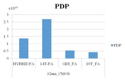
Figure 11. PDP of CMOS Full Adder Circuits
The comparison of delay between Conventional CMOS Full Adder circuits and FinFET Full Adder circuits is presented in Figure 12.
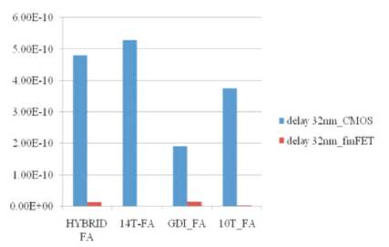
Figure 12. Comparison of Delay between Conventional CMOS and FinFET Implementation of Full Adders
In Figure 13, the comparison of average power dissipation between CMOS Full Adder circuits and FinFET Full Adder circuits is presented.
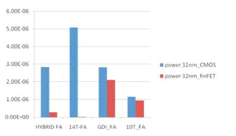
Figure 13. Comparison of Average Power Dissipation between Conventional CMOS and FinFET Implementation of Full Adders
The comparison of delay between 45 nm and 32 nm FINFET based Full Adder designs is given in Figure 14.
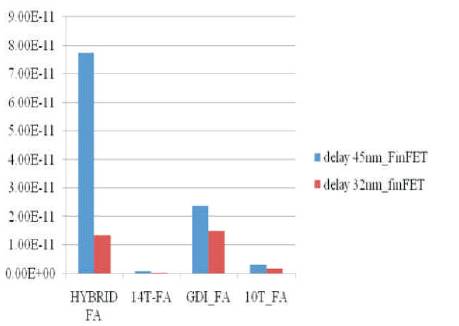
Figure 14. Comparison of Delay between 45 nm and 32 nm FINFET Implementation of Full Adders
In Figure 15, the comparison of average power dissipation between 45 nm and 32 nm FinFET Full Adder circuits is presented.
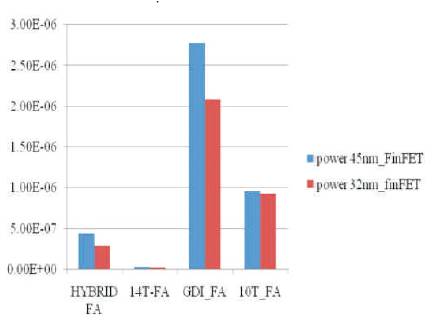
Figure 15. Comparison of Average Power Dissipation between 45 nm and 32 nm FinFET Implementation of Full Adders
The proposed FinFET based full adder designs are implemented and compared with conventional CMOS full adders. Hybrid full adder using FinFETs achieved a reduction of 97.2% in delay and 89.8% average power consumption. 14 transistor full adder using FinFET achieved 99.9% and 99.6% reduction in delay and power. GDI FA using FinFETs reduces delay and power by 92.1% and 25.8%. 10T FA using FinFETs reduces delay and power by 99.6% and 18.3%. The proposed FinFET based full adders consume less power and delay is also less compared to conventional MOS designs.
FinFET devices consume less power and low delay compared to conventional CMOS devices. By varying the fin width, fin height, doping concentrations of FinFETs, power dissipation and delay can further be optimized.