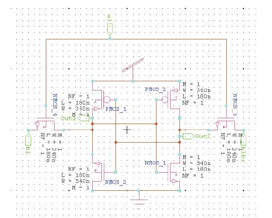
Figure 1. 6T SRAM Cell
Leakage current has been a major issue in system on chip designs with sub-micron technologies. For 180nm and below technologies, leakage is the main factor which dominates over the dynamic power and contributes to almost or more than 40% of total power dissipation. Thus it become very important to control the leakage current. This paper presents the effect of several techniques based on leakage reduction mechanism such as stacking effect and sleepy stack transistors on standard 6-T SRAM cell. Also their comparative analysis has been carried out on the basis of leakage current, propagation delay, static noise margin (SNM) and dynamic power dissipation. The produced result depicts SRAM cell with stack technique shows 16.65%increase in propagation delay, whereas sleepy stack SRAM shows 32.83% reduction in delay as compare to basic 6T SRAM cell. When we discuss about dynamic power dissipation 6T SRAM cell with stack technique consumes 39% more, but sleepy stack cell(in sleep mode) dissipates 17.61% reduced and sleepy stack cell (in active mode)dissipates 10.47% less power as compare to basic 6T SRAM cell.
About leakage current, it can be seen that 6T SRAM cell with stacking effect shows 86% less leakage flowing through the NMOS transistor whereas in PMOS transistor the leakage current got reduced to 99.94% as compare to basic 6T SRAM cell. When we come to sleepy stack technique the leakage current flowing through the NMOS cell increases by 111%, where there is a small difference in leakage of PMOS as compare to leakage of PMOS of 6T SRAM cell.
Tools Used: TANNER EDA for schematic simulation, The simulation technology used is TSMC 180nm.
As CMOS technology scales deep into nanometer regime, the density of memory bit cell has been increase significantly, resulting in larger embedded memories for the same die area. In high performance ICs about 40% of the total active power is consumed due to the leakage current(Farzan Fallah et al., 2005). It is well known that leakage is the source of energy consumption in idle state of the circuit (S. Borkar et al., 1998) .SRAM arrays are important sources of leakage because the majority of transistors are used in on chip memory in today's high performance microprocessors (Debasis Mukherjee et al., 2010). Therefore the design of low leakage SRAM cell is highly desirable.
In addition to leakage current, the degradation of speed in SRAM cells is another growing issue(Zhang, L. et al. 2011), (M. Johnson, 2002). Due to its superior performance capabilities and compatibility with the CMOS logic process, the six transistors (6T) Static Random Access Memory (SRAM) has been adopted as for many SOC embedded memories(Kaushik Roy, 2003).
6T SRAM cells with stacking effect and sleepy stack 6T SRAM cell has been discussed in this paper. The effect of these techniques has been carried out for 6T SRAM cell on the basis of leakage current, propagation delay, SNM and dynamic power dissipation. The sleepy Stack SRAM cell shows less delay as compare to other techniques. If the width of the sleep transistors got double as compare to the stack transistors taken in series in sleepy stack SRAM cell, the time taken by the cell is also get reduced.
The introduction and design of 6T SRAM is discussed in section 2.1. The 6T SRAM cell with stack technique and sleepy stack technique is introduced in section 2.2 and 2.3 respectively.
A 6T SRAM cell in 180nm CMOS technology is shown in Figure1. The storage cell is composed of two back- to-back inverters. NMOS transistors N1 and N2 are known as the driver transistors and PMOS transistors P1 and P2 are known as the load transistors (Sapna Singh et al., 2012). The transfer gate is formed by transistors N3 and N4. These are known as the access transistors. In conventional 6TSRAM cell, the stored data got distorted due the voltage division in cross coupled inverter. There are some limitations on the sizing of transistors, so that proper read and write operation can be maintained. For proper read operation, the current conducted by NMOS driver must be higher as compare to the access transistors. And for write operation, the current conducted by the access transistors must be stronger as compare to PMOS load transistors. For proper read and write operation the W/L ratio of access, driver and load transistor of 6T SRAM cell is shown in Table 1.
Figure 1. 6T SRAM Cell
Table 1. W/L Ratio of 6T SRAM
In 6T SRAM cell, there are two storing nodes out1 and out2. If “1'' is stored at the node out1 and “0'' is stored at node out2, at this moment transistor PMOS_1 and NMOS_2 are in cutoff state and the leakage current will flow through these two transistors. The leakage current is shown in Table 2.
The 6T SRAM with Stack effect is shown in Figure 2. The stack effect is used when the memory is in ideal mode. The stack transistors implemented in the circuit reduce leakage current, when two or more stacked transistors are turned off together. These off transistors induced reverse bias between them, results in leakage current reduction (Gholamreza Karimi et al., 2011) (G. Razavipour et al, 2009)]. The limitation of this technique is that it increases the propagation delay of the circuit.
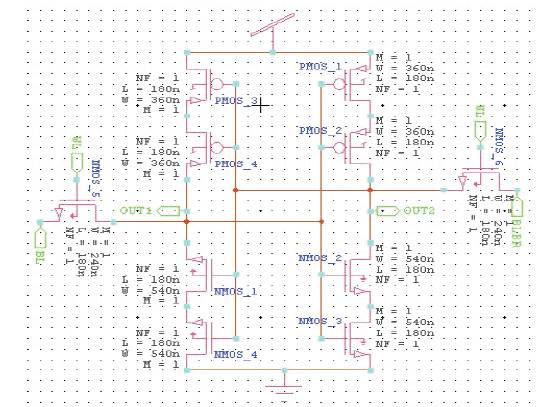
Figure 2. 6T SRAM Cell Using Stack Technique
In this technique instead of one NMOS and one PMOS in inverter, stack is formed by adding one more transistor with each one. The W/L ratio of the stack transistors are shown in Table 2. Instead of dividing the width of the stack it remained same, and the effect is observed on the leakage current. The leakage current is shown in Table 4.
Table 2. W/L Ratio of SRAM Using Stack
In sleepy stack technique, sleep transistors are added to 6T SRAM stack. The 6T SRAM cell with sleepy stack is shown in Figure 3. The W/L ratio of the cell is shown in Table 3.
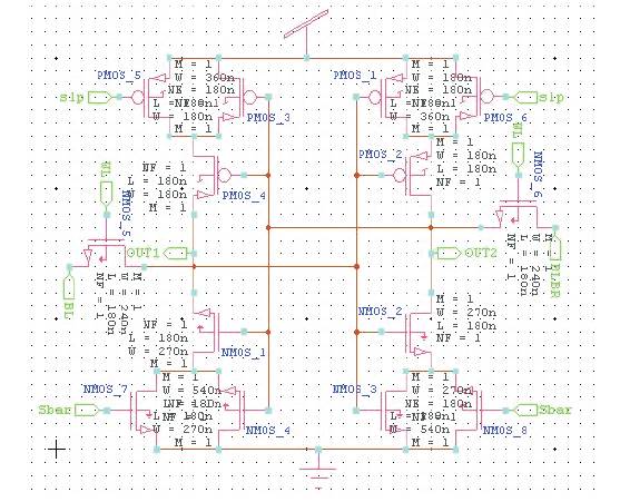
Figure 3. 6T SRAM Cell Using Sleepy Stack Technique
During active mode, sleep transistors are ON, then reduced resistance and increases the current while reducing delay. During sleep mode, sleep transistors are OFF, stacked transistors suppress leakage current (Harsh Raj et al., 2014). When all sleep transistors are OFF, the cell goes into the sleep mode so the leakage current decreases. Whereas in active mode of the cell, the leakage current increases as compare to the sleep mode of the cell but the advantage of 32.83%less delay as compare to basic 6T SRAM cell .
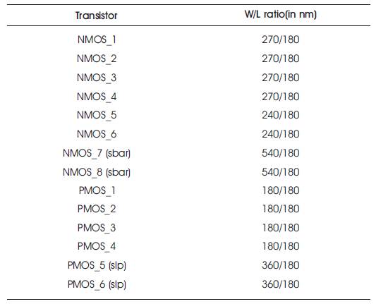
Table 3. W/L Ratio of Sleepy Stack SRAM
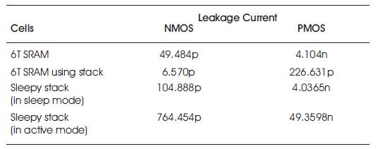
Table 4. Comparison of Leakage Current of Different SRAM Cells
The SNM is defined as the “maximum amount of noise voltage that can be introduced at the output of the two inverters, such that the cell remain in the same state, means that the stored data should not change ” (E. Seevinck et al.,1987). SNM calculate the amount of noise voltage required at the internal nodes of the SRAM cell to flip the cell data (Deependra Singh Rajput et al., 2012). SNM can be calculated by the use of butterfly curve method. Figure 4 shows the butterfly curve for basic 6TSRAM cell. The Figure 4 plots the voltage transfer characteristic (VTC) from Inverter 2 and the inverse VTC from Inverter 1. The resulting curve is called a “butterfly curve” and is used to determine the SNM.
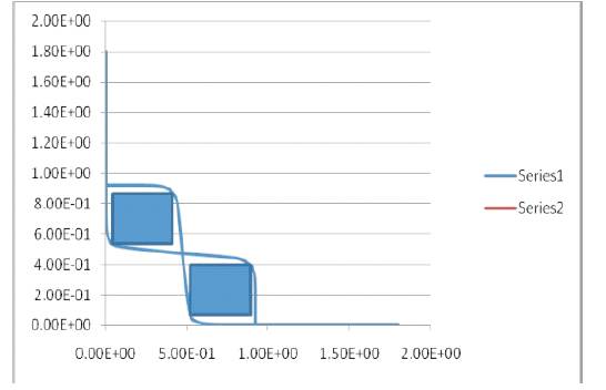
Figure 4. Butterfly Curve for SNM of 6T SRAM Cell
The butterfly curves of SRAM cell using stack technique and sleepy stack technique also approximately same, because the SNM do not get affected by these techniques.
In this section, the authors estimated the impact of stack technique and sleepy stack technique on 6T SRAM cell on the basis of leakage current, delay, dynamic power dissipation and static noise margin. The circuit is characterized by using the180nm technology with the supply voltage of 1.8 volt. Circuit verification is done on the Tanner tool. Schematic of the SRAM cell is designed on the S-Edit and net list simulation done by using T-spice and waveforms are analyzed through the W-edit.
Table 4 shows the comparison of leakage current for different cells, it can be seen that 6T SRAM cell with stacking effect shows 86% less leakage flowing through the NMOS transistor whereas in PMOS transistor the leakage current got reduced to 99.94% as compare to basic 6T SRAM cell. In sleepy stack technique, the leakage current flowing through the NMOS cell increases by 111%, where there is a small difference in leakage of PMOS as compare to leakage of PMOS of 6T SRAM cell. Figure 5 gives the graphical representation of leakage current flowing through the different SRAM cells.
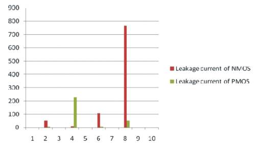
Figure 5. Comparison Graph of Leakage Current of Different SRAM Cells
In Table 5 the comparison of propagation delay, dynamic power and static noise margin has been shown. SRAM cell with stack technique shows 16.65%increase in propagation delay, whereas sleepy stack SRAM shows 32.83% reduction in delay as compare to basic 6T SRAM cell. When we discuss about dynamic power dissipation 6T SRAM cell with stack technique consumes 39% more, but sleepy stack cell(in sleep mode) dissipates 17.61% reduced and sleepy stack cell (in active mode)dissipates 10.47% less power as compare to basic 6T SRAM cell.
Figure 6 shows the graph for the comparison propagation delay, dynamic power and static noise margin.
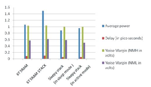
Figure 6. Comparison Graph of Average Power Dissipation, Propagation Delay and Noise Margin
With Scaling down the feature size of the CMOS transistor the leakage current has been increased tremendously. In this paper, the authors have presented techniques called Stack effect and sleepy stack technique, which can achieve more leakage current reduction as compare to the basic 6T SRAM cell. In stack technique, beside leakage reduction there is a drawback of delay penalty as compare to 6T SRAM cell. Whereas sleepy stack technique reduces leakage current as well as shows the less delay of 56.82 pico seconds.
This paper reveals that the leakage current has been reduced with great margin in 6T SRAM cell using stack technique cell but at the cost of propagation delay, in this case the delay increases by16.65%. Designing 6T SRAM cell with sleepy stack technique could further increases the leakage current however the advantage of this technique is that in active mode it reduces the delay by 32.83% as compare to 6T SRAM cell and shows 42.42% less delay as compare to SRAM cell using stack technique.