An Energy Efficient Tri State Buffer Logic Using
Subthreshold Adiabatic
M. Bharathi
Assistant Professor, Department of ECE, Sree
Vidyanikethan Engineering College, Tirupathi.
Abstract
Tristate buffer is used in many applications such as electronics,
communications and microprocessor circuits where they
allow many devices to be connected to the same wire or bus without damage
or loss of information. Contention occurs,
if multiple devices are connected to same data bus. In general, digital
information can be sent either serially or in
parallel. For example, in microprocessor, information can be sent through
data high way buses which allow multiple
Tristate buffers to be connected together without loss of information. In
general, buffer not only provides isolation, but
also used to provide current or voltage amplification to drive heavy
loads. These Tristate buffer devices can be used as
bidirectional switches, because they are constructed using MOSFETS. This
paper provides an energy efficient tristate
buffer which is implemented using static CMOS, adiabatic and two
Subthreshold adiabatic in HSPICE using 0.18μm
CMOS standard process technology. The results obtained in the paper is
effective in terms of power and area.
Keywords :
- Tristate Buffer,
- CMOS Logic,
- Adiabatic logic,
- Subthreshold Adiabatic Logic,
- HSPICE.
Introduction
Energy harvesting is a technique that captures power
supply, such as a small energy that occurs due to vibration,
heat dissipation, and electromagnetic field. This technique
is to be useful for making some applications like health
monitoring implant, and building automation. However,
the energy obtained from power resources is weak, and
also the value of voltage or current is low-level, so that the
logic circuit for energy harvesting is required to more
reduce the power consumption. In order to achieve the
lower power consumption, we may consider two existing
low-power technologies, sub-threshold CMOS theory, and
an adiabatic logic circuit technology. Sub-threshold CMOS
theory is a technique which can reduce the power
consumption to lower than threshold voltage. On the other
hand, adiabatic logic circuits is a technique that varied the
slope of the constant voltage power supply, and it reduces
energy consumption by suppressing the voltage applied to
the resistance of the circuit.
(Kazunari Kato, Yasuhiro
Takahashi, and Toshikazu Sekine, 2014).
An adiabatic
system consists of two main parts, one is the digital core
design made up of adiabatic gates and secondly the
generator of the powered clocked signals. The power- clock generation is
most important topic in adiabatic
systems, as an efficient generation of the different phases
making up the power-clock is essential to get high overall
saving factors (Fundamentals of Adiabatic logic-Springer
Publications).
In today's CMOS technologies variations in the process are
a major concern, circuit designers are confronted with new
ideas in designing robust circuits. Also in Adiabatic Logic,
process variations have an impact on the circuit, mainly
the energy consumption.
1. Subthreshold Adiabatic Logic Circuit
The MOS transistor conducts for voltages below the
threshold voltage. This effect is called “subthreshold” or
“weak-inversion” conduction. This confirms that the current
does not drops to zero immediately even for Vgs< Vt, but
actually decays in an exponential manner, as that of a
bipolar transistor. A sub-threshold adiabatic logic circuit,
the proposed circuit, uses two power Supplies which has
different frequencies and amplitude power supplies, and
therefore the power consumption of proposed logic can
be reduced.
The Two Phase Clocking Subthreshold Adiabatic Logic,
(Kazunari Kato, Yasuhiro Takahashi, and Toshikazu Sekine,
2014) uses a two phase clocking power supply which uses
two different frequency and amplitude. For example, a 2-
chain inverter circuit is shown in Figure 1. The timing chart for
the circuit is shown in Figure 2. It is necessary to switch on-off
the input signal when Vpc and  . The frequency of is
twice, based on the frequency of Vpc and the input signal
frequency is 1/2. The amplitude of Vpc and are 0–0.5V
and 0–0.25V respectively. The frequencies of Vpc and
are
10kHz and 20kHz. In period of T2, T4, T6 and T8, the voltage
of these power supplies is low level and therefore, the
outputs are always low-level; this means these timing
become read protection period
(Tungamounika, Duvvuri
Praveen, M.Bharathi (2014)
.
. The frequency of is
twice, based on the frequency of Vpc and the input signal
frequency is 1/2. The amplitude of Vpc and are 0–0.5V
and 0–0.25V respectively. The frequencies of Vpc and
are
10kHz and 20kHz. In period of T2, T4, T6 and T8, the voltage
of these power supplies is low level and therefore, the
outputs are always low-level; this means these timing
become read protection period
(Tungamounika, Duvvuri
Praveen, M.Bharathi (2014)
.
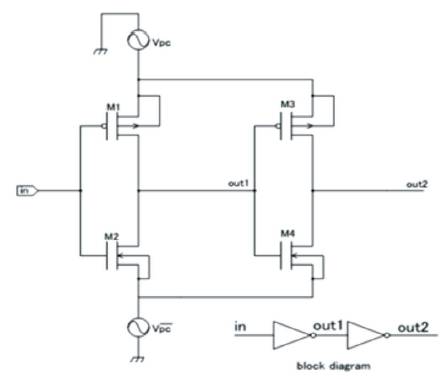
Figure 1. Cascaded inverter
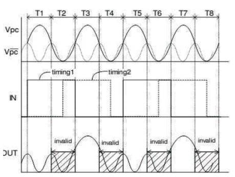
Figure 2. Timing chart for inverter
2. Tristate Logic
In digital electronic circuits, we need to isolate logic gates from
one other or have them drive or switch higher than
normal loads, such as relays, solenoids and lamps without
the need for inversion. One type of single input logic gate
that allows us to do just that is called the Buffer
(http://en.wikipedia.org/wiki/Three-state_logic).
Therefore a
buffer is a circuit also known as “non-inverting” device
which produces the output same as input. As shown in
Figure 3, tristate or three state logic allows an output to be in
logic '0', logic '1' or High impedance (http://www.
electronicstutorials.ws/logic/logic9.html.)
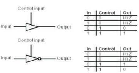
Figure 3. Symbols and logic table for Tristate non
inverting
and inverting buffer
Figure 4 and Figure 5 are implemented in static CMOS,
adiabatic and Subthreshold adiabatic using two phase.
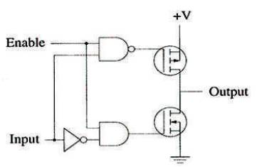
Figure 4. Logic circuit of Tristate Non Inverting
Buffer
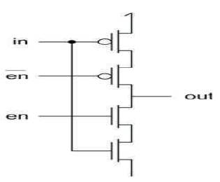
Figure 5. Logic circuit of tristate inverting
buffer
3. Simulation Results & Discussion
In this section, Figures 6, 7, 8, 9, 10 &11,are showing the
simulation results for tristate buffer and inverter using CMOS,
ADIABATIC and sub threshold adiabatic logic using two
phase clocking.
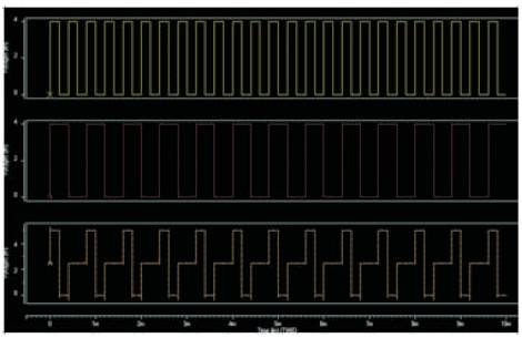
Figure 6. Timing chart for Tristate buffer using
CMOS
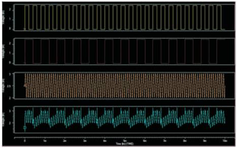
Figure 7. Timing chart for Tristate buffer using
adiabatic
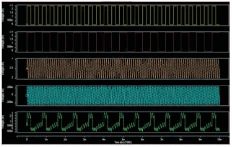
Figure 8. Timing chart for Tristate buffer using two
phase clocking
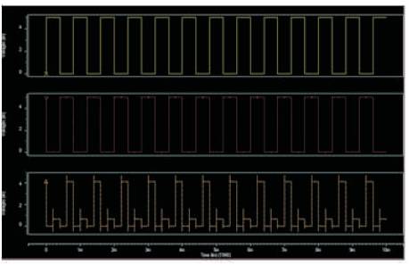
Figure 9. Timing chart for Tristate Non inverting
buffer using CMOS
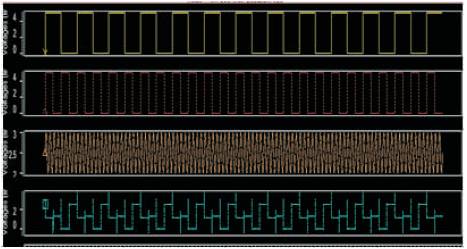
Figure 10. Timing chart for Tristate Non inverting
buffer using Adiabatic
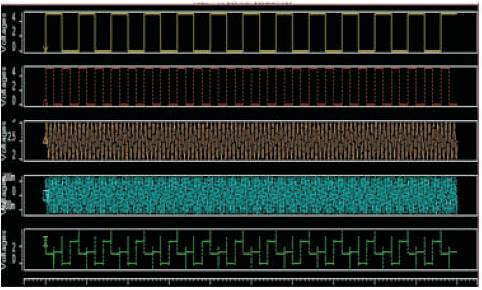
Figure 11. Timing chart for Tristate Non inverting
buffer using Adiabatic
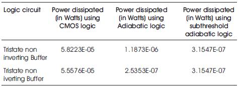
Table 1. Power dissipation of inverting and non
inverting
Tristate buffer logic
Conclusion
In this paper, the author has proposed a Tristate non inverting and
inverting buffer using Static CMOS, adiabatic and sub threshold adiabatic
logic. As the name implies
Static CMOS used static power supply. Adiabatic logic
circuit uses a sinusoidal supply at VDD, whereas sub
threshold circuit uses two different frequency and
amplitude power supply. Then the analysis are performed
for functional verification of circuits using SPICE simulation
and also power dissipation is compared as shown in Table
1. These can be also used as Bidirectional switches as it is
implemented using MOS Devices.
References
[1]. Tunga mounika, Duvvuri Praveen and M.Bharathi (2014).
“An Efficient Low Power Multiplier Using
subthreshold Adiabatic Logic”, i-manager's Journal on
Circuits and Systems, Vol. 2(3) June - August 2014, Print ISSN-
2321-7502, E-ISSN 2322-035X, pp. 29-32.
[2]. Kazunari Kato, Yasuhiro Takahashi, and Toshikazu
Sekine (2014). “Two Phase Clocking Subthreshold
Adiabatic Logic”, Proc. IEEE, pp. 598-601.
[3]. Fundamentals of Adiabatic logic-Springer Publications
[4]. http://en.wikipedia.org/wiki/Three-state_logic
[5]. http://www.electronicstutorials.ws/logic/logic9.html