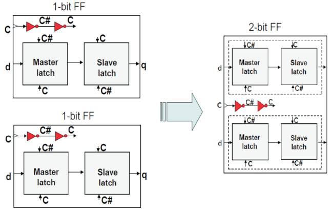
Figure 1. Merging two one bit flip-flop into two bit flip-flop (a)two 1-bit flip-flop [before merging] (b) 2-bit flip-flop[after merging].
Power reduction is a main parameter to design VLSI circuits. In this paper, to design a number of D-flip flop performing at the same time, the given clock signal is reduced using multi bit flip-flop. The multi bit flip flop is mainly used to improve the clock power for the given common clock signal and to reduce the switching power. This method is performed to replace some D flip-flop into multi bit flip-flops with the given common clock input. In this proposed technique, first step is to identify the flip flops and its placed location, second step is to build the combination table mainly by merging the flip flop and removing the unwanted merging flip-flops, final step is to assign the region , place the flip flop in these flip-flops merging and replacing the merging location. By using this method, the result is used to reduce the power to 24mW and area by reducing to 35 gate count ,because this method considers the area measured as the number of gate count in the merging flip flop.
In VLSI (Very Large Scale Integration), construction of the chip design depends upon the switching power and interconnection of the clock power. Recently using flip-flop design based chip, it consumes 20-40% of clock power and the design depends upon the flip-flop distributing the clock power or replacement of one with another.
In design based flip-flop, the clock is configured in 3 ways, to asserting the clock is level triggered, changing the state of the clock is edge triggered, and the transfer from one edge to another edge, i.e. master-slave flip-flop.
The previous work was performed by using the multi bit flipflop concept applying the post placement stage. In this method, graph based approach algorithm was used. One node represent the flip-flop and two 1-bit D flip-flops were considered, then replaced by new two one bit flip-flops without clock timing which then builds the edge between corresponding flip-flops. Some drawbacks occurred by using MBFF in post placement stage. They are,
It's performance is based on increasing the wire length to build the edge between those corresponding flip-flops.
Multi bit flip-flop very effectively saves the power and area by implementing the method of merging the single bit flipflops in design. By using Multi Bit Flip-Flop [MBFF] concept in order to reduce the clock and switching power, the total flip-flop area is also reduced effectively[1,2].
Figure1(a) shows the two 1-bit flip-flop performed before merging but after using multi bit flip-flop concept to merge the two one bit flip-flops into a two bit flip-flop is shown in Figure 1(b). It's based by combining two 1-bit flip-flop into two bit flip-flop reducing the two inverters.
Figure 1. Merging two one bit flip-flop into two bit flip-flop (a)two 1-bit flip-flop [before merging] (b) 2-bit flip-flop[after merging].
The proposed method is based on the following flowcharts given (Figure 2).
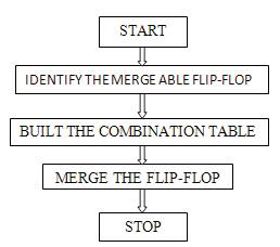
Figure 2. Flow chart of proposed method
In this section by considering the legal placement Region R(f1 ) and R (f2 ) and assigning two 1-bit flip-flops giving input p1 & p3 the outputs p2 & p4 are obtained.
Interconnect the two one bit flip-flops. That merging place is identified by the dotted lines (R3 ) and this diamond shape is the proper location to place the merging flip-flop (Figure 3a & 3b).
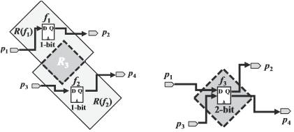
Figure 3. (a) R(f1) and R(f2) are Legal placement region of flip-flop f1 and f2 and R3 is feasible area at the region of R(f1) and R(f2). (b) Merging new flip-flop f3 used to replace flip-flop f1 and f2 without effect timing for pins of p1,p2,p3, and p4.
For this, a library is assigned where (Figure 4 (a)(b)(c)(d)(e) and (f)) type1 is 1-bit and type2 is 4-bit as considered and a combination table is assigned where T n1 is 1-bit and n2 is 4-bit (A). Pseudo type bit is added to help the merging of flip-flop in combination table T and is assigned tree for 1 and 4-bit (B).Combination is as shown In Figure 4.
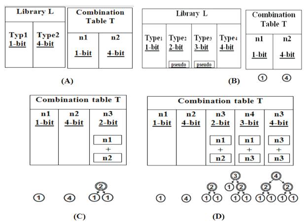
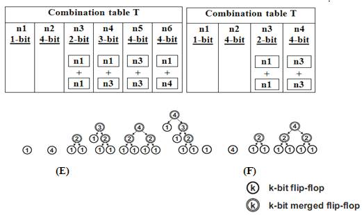
Figure 4. (A) Initially the library L and combination table T. (B) Adding pseudo type in library L and assign binary tree in combination table T. (C) create new combination obtained to merging n1 & n2. (D) another two new combination obtained to merging the node n1, n2 and n3. (E) obtained new one to get the combination of n1 & n4. (F) finally the combination table obtained perfect combination after removing impossible combination I n figure 4 (E).
Table T merges two n1 & replace into n3( c ). In the same way, n1 and n3 into n4 are merged also n3 and n3 into n5 (D), n1and n4 are merged into n6 (E).
Finally, the unwanted combination is removed and final possible combination Table T (F) is get the Advantage of removing combination table, which is the removed unused combination which helps in the merging of flipflops.
Merge flip-flop (Figure 5(a)(b)(c)(d)(e),(f)) is performed in the following ways (a) divide a chip into several sub-regions and assign 1-bit flip-flop f1 and f2 (b) flip-flop f1 and f2 are merged and replaced getting new bit f3 at n4 (c) assign flip-flop f6 and f5 merge and replace getting new bit f6 at n4 (d) assign 2-bit flip-flop f7 and f8 [4,5].
Merge and replace into new bit fq at h5 (e) 2-bit flip-flop and merge and replace into new bit f3 at h5 (f) completely merging and replacing flip-flops.
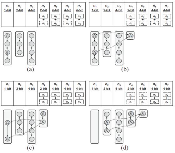
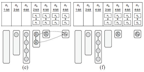
Figure 5. Replacement of flip-flops (a) set flip-flop in sub-region before merge (b) two 1-bit flip-flop f1 and f2 merge and replace into the region f3. (c) two 1-bit flip-flop f4 and f5 merge and replace into the region (d) two 2-bit flip-flop f7 and f8 merge and replace into the region (e) two 2-bit flip-flop f3 and f6 merge and replace into the region f10 (f) finally to get after merging flip-flops.
Xilinx ISE 13.2 and Model sim 8.1c software is used to implement the method. The output is two one bit flip-flops when separate clock pulses are given. Figure 6 shows Power and Area Reduction before Merging.
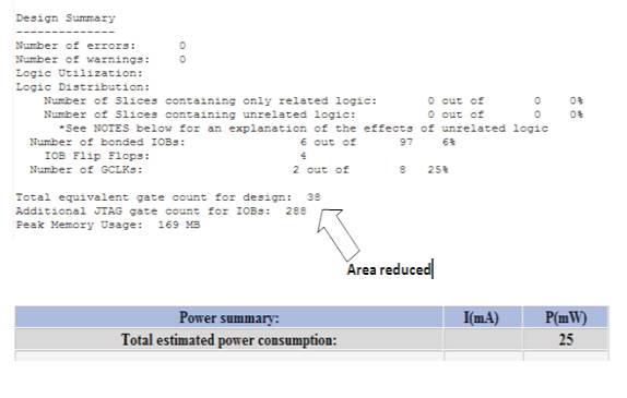
Figure 6. Power and Area Reduction before Merging
In proposed work, the two 1-bit flip-flops merge and when common clock pulse is given, the output is obtained as that is based on given output given in Figure 7[6,7,8,9 ].
Using the Model sim 8.1c to merge and replace the flipflops and get the simulation result as given below, the simulation results depend upon the combination table and the merging and replacement of flip-flop[13]. (Figure 8)
Tables 1 and 2 show the comparison of the existing method and the proposed method .
Its reduced power and area are clearly shown in the graphical representations (Figure 9 and 10).
These comparisons show that the proposed method effectively reduced the power and area of gate count.
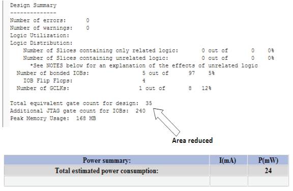
Figure 7. Power and Area Reduction after Merging
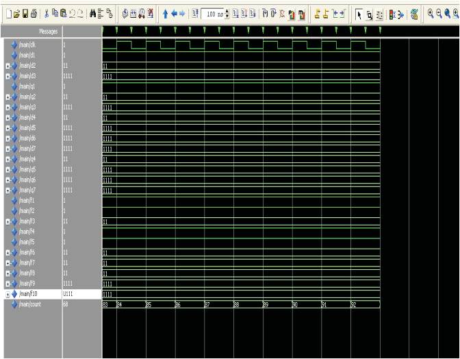
Figure 8. Simulation Result to implementation of flip-flop
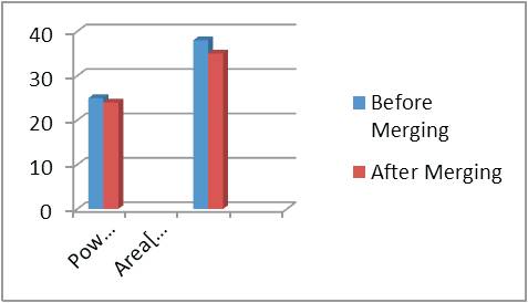
Figure 9. Graphical representation of our proposed Method
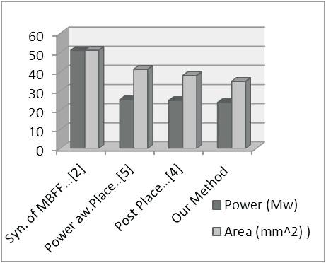
Figure 10. Graphical representation result with reference papers
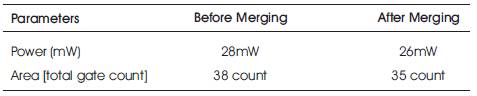
Table 1. Comparison table in area & power
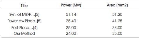
Table 2. Comparison table of our results with reference papers
In this proposed method, the authors have merged the D flip-flops for reducing the switching power in VLSI design. Using this multi bit flip-flop, switching power can be reduced and the clock power can be improved [14]. This method is performed to identify the flip-flop and the combination table is built by merging the possible combination and then replacement of flip-flop, placing it in the proper location. This concept is used to reduce the switching power to 24mW and reduce the area depending upon gate count to 35. In future work, this method will be used to design the counter and shift register so that the, delay can be reduced.
The authors would like to thank beloved Principal and Management of Paavai Engineering College, Namakkal for giving excellent computer and lab facilities.