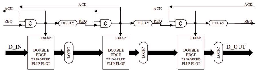
Figure 1. FIFO Sequencer (Gupta, et al., 2012)
In this paper, Positive Feedback Source Coupled Logic (PFSCL) based asynchronous pipeline implementation is addressed. Existing Conventional PFSCL and a more efficient Triple-Tail Cell-based PFSCL variant are used for this purpose. Striking a trade-off between both topologies, a new hybrid implementation of the pipeline has been proposed. The concept is elucidated through FIFO sequencer. The hybrid implementation of asynchronous pipeline results in lesser number of gates as well as lower average power dissipation, thus not only making the circuit more efficient but also reducing overall area overhead. The validity of the proposal is confirmed through SPICE simulations using 0.18 um CMOS technology parameters.
Pipelining refers to the execution of a number of instructions simultaneously with each instruction present at a different processing stage (Allan, Jones, Lee, & Allan, 1995) . It enhances the performance of the system by increasing the number of instructions being processed in a given machine cycle without affecting clock frequency (Nowick, 2011). The number of simultaneous instructions being executed augments with the number of pipeline stages which ameliorates throughput. From numerous taxonomies, pipelines are broadly classified into synchronous and asynchronous counterparts.
A synchronous pipeline has all its components, governed by a single global clock, whereas in an asynchronous pipeline, all components are self-governed using various handshake protocols to communicate (Sjogren & Myers, 2000) (Yun, Beerel, & Arceo, n.d.). Both counterparts have their own set of advantages and disadvantages. The upside of asynchronous pipelines being that they are independent of the problem of clock skew and global timing issues (Gupta, Pandey, & Gupta, 2012). In this paper, a FIFO sequencer is used to illustrate asynchronous pipeline functionality. It follows dual rail encoding with two-phase handshaking protocol in order to achieve synchronism (Nowick, 2011; Saxena, Dutta, & Pandey, 2016) .
Conventionally, digital circuits were realized using CMOS logic family because of their negligible static power dissipation and convenience of design (Kang & Leblebici, 2003; Rabaey, Chandrakasan, & Nikolic, 2003) . However, due to their vulnerability to noise and relatively high mismatch in CMOS devices, newer logic families such as Source-Coupled Logic (SCL) and PFSCL are suggested in the literature. Source-Coupled Logic (SCL) family is an efficient alternative due to its high-speed implementations of various circuits (Gupta, Sridhar, & Chaudhary, 2011; Allstot, San-Hwa Chee, Kiaei, & Shrivastawa, 1993) . The fast operation of this logic family is because of increased bias current (Musa & Shams, 2010; Alioto & Palumbo, 2003).
Source-Coupled Logic with Positive feedback (abbreviated as PFSCL), one of the recently evolved variants of SCL, acquiesces us to have superior speed as compared to traditional source-coupled logic (Gupta, et al., 2011; Alioto, et al., 2005). The high speed of PFSCL circuits is ensured by diminished aspect ratios, causing parasitic capacitances to reduce the latency of employed NMOS transistors. The nature of feedback is positive because the output is used to drive the gate of the NMOS transistor. It is fundamentally a single ended SCL topology which replaces the reference voltage source, like in conventional SCL (Alioto, et al., 2005). Triple-Tail Cell model, another upgraded variant of the PFSCL helps in reducing power dissipation, as it lowers the number of current sources (Kimura, 1995; Gupta, Pandey, & Gupta, 2013; Pandey, Gupta, & Gupta, 2014) as compared to PFSCL.
Firstly, this paper describes the pipeline architecture (design of FIFO sequencer) and its important elements, DETFF (Double-Edge Triggered Flip Flop) and C-Muller element form the prerequisites for its implementation (Gupta, et al., 2012; Rabaey, et al., 2003). Secondly, two variants of PFSCL, conventional PFSCL, and Triple-Tail Cell-based PFSCL have been discussed in detail and also used to implement the pipeline later. Furthermore, a trade-off between the two topologies has been made to propose a hybrid implementation of the pipeline, combining both conventional and Triple-Tail Cell-based PFSCL. Finally, a thorough analysis of all three implementations has been presented comparing various characteristic parameters showing the advantages of the proposed hybrid topology.
The concept of asynchronous pipeline was pioneered by David Muller in 1963. The concept involves use of certain encoding schemes and handshaking protocols in order to obtain synchronism among various components. The two handshake signals are Request and Acknowledge, among which request signal helps to keep synchronism with next stage of the pipeline and acknowledge signal, with the previous stage (Nowick, 2011). In two-phase handshaking protocol, any voltage level change, be it high to low or low to high is considered as a valid state. There is no resetting of signals once a transition from one valid state to another takes place whereas, in the case of four phase handshaking protocol, only the signal level change from low to high is considered as a valid state. The signals are reset to a low-level each time before sending data forward. A typical digital circuit known as FIFO sequencer has been used to simulate the working of an asynchronous pipeline in this paper. FIFO sequencer follows single rail encoding and two-phase handshaking protocol (Nowick, 2011; Saxena, et al., 2016) to establish synchronism.
A FIFO sequencer has been implemented in this paper (Nowick, 2011). It shows the functioning of an asynchronous static pipeline using two-phase handshaking protocol and single rail encoding of bits. A pipeline consists of three basic elements, a latch to control the flow of data, data element with its logic and its control circuit. The control circuit is comprised of a C-Muller element whose output acts as an enable signal for the Double-Edge Triggered Flip-Flop (DETFF). DETFF provides the functionality to latch data for a period of time until desired handshaking signals are established to further the pipeline's operation. FIFO's components including C-Muller element, Double-Edge Triggered Flip-Flop (DETFF) and an inverter have been designed using Positive Feedback Source-Coupled Logic (PFSCL) and Triple-Tail Cell-based PFSCL (Gupta, et al., 2012).
To briefly understand FIFO sequencer's working and analyze how synchronism is established, a single pipeline stage is considered (let's say the middle stage shown in Figure 1). The handshake signals used include REQ, which is sent by the previous stage denoting the presence of new data element available at its output and ACK, which is sent by the next stage indicating successful latching of previous data element sent by this stage. These two signals are fed as inputs to C-Muller element, corresponding to the stage under observation and accordingly enable signal for DETFF (latch) is generated. Once DETFF is enabled, it becomes transparent hence, allowing DIN at its input to pass through itself such that it replaces previous value of DOUT. Then DOUT passes through the logic block, following the pipeline stage and generating DIN signal for next stage. Consequently, C-Muller's output is used to generate and send REQ signal for the next stage and ACK signal for the previous stage. Whenever DETFF is not enabled or becomes opaque, it retains the value at its output, taking no notice of DIN until it's enabled. The delay element provided in this circuit for REQ signal is important for both, the inverted ACK signal and delayed REQ signal to reach the input of C-Muller element simultaneously, which is seminal for proper functioning of C-Muller element (Gupta, et al., 2012)
Figure 1. FIFO Sequencer (Gupta, et al., 2012)
The C-Muller element is an asynchronous sequential element, which generates the enable signal required for proper functioning of Double-Edge triggered flip-flop. It works in accordance with the truth table of Table 1 as it latches to previous output values for different inputs. The CMuller element is designed and implemented using an AND gate, NOR gate and a S-R latch as shown in Figure 2 (Rabaey, et al., 2003). When inputs A and B are same, the output is same as both the inputs. When inputs are different, output retains its value from the previous state, this explains the use of S-R latch. The entire circuit can be summarized using the Boolean function -
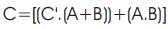
Where, C is the present output, C̅ is complement of the present output, C' is the previous output value and A, B are the inputs.
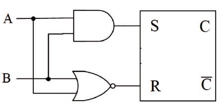
Figure 2. C-Muller Circuit (Rabaey, et al., 2003)
Table 1. Truth Table of C-Muller Element
The DETFF is another vital component for implementing a FIFO sequencer, as it stores new data produced by the logic unit until, the subsequent stage is ready to receive it (Gupta, et al., 2012). It is named Double-Edge triggered as it functions at both, rising and falling edges of the local strobe signals. The block diagram of DETFF, as shown in Figure 3, consists of a multiplexer and two D-latches (gate level implementation is shown in Figure 4). The two DLatches are enabled alternatively with the outputs being fed to a Multiplexer, which is enabled by the same strobe pulse used to enable the D-latches. Hence, the multiplexer selects the output of one of these latches when enable signal is high and output of the other latch when it is low. When the clock (CLK) is high, LATCH L1 becomes transparent holding the current data input and the previously stored data in LATCH L2 appear at the output. Consequently, when CLK is low, LATCH L2 becomes transparent and data stored in LATCH L1 during the previous state is obtained as the output.
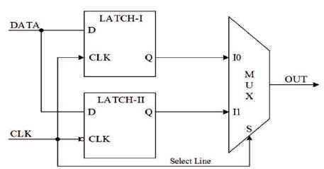
Figure 3. DETFF Block Diagram (Gupta, et al., 2012)
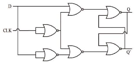
Figure 4. D-latch using NOR Gates
The primary objective of this paper is to evaluate asynchronous pipeline's implementation using two different PFSCL topologies that are conventional PFCL and its variant, Triple-Tail based PFSCL. These two PFSCL topologies are explicated in the following subsections.
In PFSCL, the gate of one NMOS is driven by the output voltage itself hence, the name positive feedback. This helps in achieving higher speeds than the conventional Source Coupled Logic (Alioto, et al., 2005) and permits the circuit to function with very low Power-Delay Product. The most important aspect of PFSCL implementation is the calculation of width to length ratio which has a seminal impact on the performance characteristics of this logic family. The calculations were done for VSWING equal to 400 mV and Iss as 100 μA, typical values are assumed for the constants involved, resulting in WN equal to 0.564 μ (width) and LN as 0.18 μ (length) (Alioto, et al., 2005). The implementation of an inverter and the two universal gates, NAND and NOR using PFSCL are shown in Figures 5 (a), (b) and (c).
To elucidate the working of PFSCL, let's consider the NOR gate as shown in Figure 5(b). When any one of the inputs is high, the corresponding NMOS transistor turns ON and conducts, making current flow through that branch (or half current flows through if one of them is ON). Now, the voltage given as feedback to the MF NMOS is low, which will turn OFF the feedback transistor. Hence, output voltage obtained is low, complying with the desired NOR gate output. Similarly, the working of NAND and NOT gates can be explained using PFSCL (Alioto, et al., 2005). Keeping the above considerations in mind and the three gates NAND, NOR and NOT, components of a FIFO Sequencer, C-Muller, and Double-Edge triggered Flip-Flop described in the previous section are redesigned using PFSCL logic.
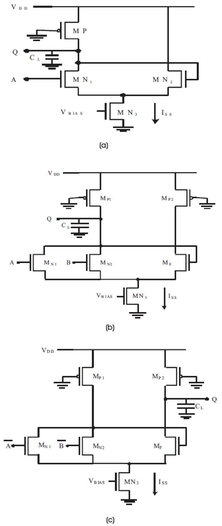
Figure 5 (a) PFSCL Inverter, (b) PFSCL NOR Gate, (c) PFSCL NAND Gate (Pandey, et al., 2014)
Triple-Tail Cell-based PFSCL is an extension of the PFSCL logic family. This variant of PFSCL allows us to have even higher speeds and enormously reduced latency compared to others. It is established around a unique fundamental cell as shown in Figure 6. The fundamental cell consists of triple tails (three transistors) each of them sharing a current source of Iss/2 (Pandey, et al., 2014). It has two triple-tail cells (Mx5, Mx6, Mx8) and (Mx3, Mx4, Mx7). The fundamental cell can be understood by considering the AND gate designed using it, as shown in Figure 6. Inputs are given to one of the transistors (Mx3, Mx5), the second set of transistors (Mx4, Mx6) provide with positive output feedback. The middle transistors (Mx7, Mx8) constitute the tail and their purpose is to be able to draw maximum bias current such that the remaining two transistors are completely switched off when the input to any one of them is high. For this reason, the aspect ratio of the third transistor (middle transistor) in both tails must be larger than the remaining two transistors so that, it is able to drive other transistors to their cut-off regions. This forms the fundamental cell whose inputs can be manipulated to obtain the functionality of various gates. The transistors (Mx7, Mx8) are given CLKBAR and CLK input respectively to drive them alternatively. When CLK is high, one triple tail works while the other is off and vice-versa when CLK is low.
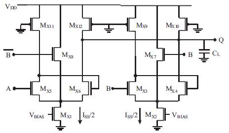
Figure 6. Triple-Tail Cell-based AND Gate Implementation (Pandey, et al., 2014)
The Triple-Tail AND gate is demonstrated in Figure 6 which works in a similar way as described above. Considering the case when B is high and A is also high, then Mx7 is ON but Mx8 is Off, therefore Mx4 and Mx6 are Off. As output voltage is given by the formula VDD-RD [ID6 +ID4], the current through both these transistors is zero. Since, ID5 =Iss/2(1+N) and ID8 =Iss*N/2(1+N), using ID5+ID6+ID8 =Iss/2 we get ID6=0, also as ID4+ID5+ID6 =Iss/2, this implies that ID4=0. Therefore, the output voltage is equal to VDD . Similarly, the working can be proved for other cases too (Pandey, et al., 2014).
Now, considering the D-latch as shown in Figure 7, let's analyze a case where D input is high and CLK is also high meaning, Mx7 is ON driving Mx4 to its cut-off state and also, high D input drives Mx6 to cut-off state, thus making output Q high. Further, when CLK is low, Mx7 is off, Mx8 is on, drawing all the current and driving Mx6 into cut-off, which leads to Mx3 turning on and cutting off Mx4, which leads to retention of the previous output value irrespective of the D input hence, validating the latching property. Similarly, other cases can be explained easily.
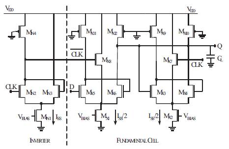
Figure 7. D-Latch Implementation using Triple-Tail Cell-based PFSCL (Pandey, et al., 2014)
In this section, FIFO sequencer's implementation using conventional PFSCL and Triple-Tail based PFSCL have been described briefly and a hybrid PFSCL topology has been proposed.
The conventional PFSCL implementation uses NOR-based architecture. All components of C-Muller element, NOR gate, AND gate and SR latch have been implemented using PFSCL NOR gates. The complete conventional PFSCL based C-Muller is shown in Figure 8. The DETFF's components (as shown in Figure 4), D-latch (for NOR-based realization refer Figure 3), and Multiplexer have been also implemented using PFSCL NOR gates.
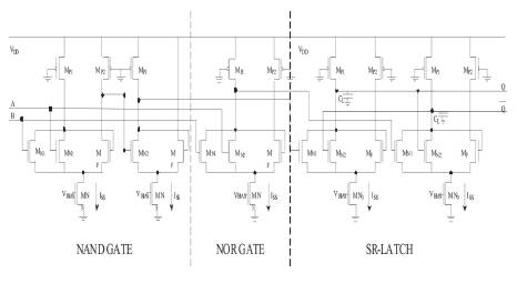
Figure 8. C-Muller Implementation using PFSCL
In Triple-Tail Cell-based architecture, C-Muller and DETFF are implemented using the fundamental cell based blocks of AND gate and D-latch. The AND gate has been manipulated to simulate C-Muller element (Gupta, et al., 2013; Pandey, et al., 2014) whereas, Triple-Tail Cell-based D-latch is modified to obtain a multiplexer which is further combined with two D-latches to obtain the desired functionalities of DETFF. The multiplexer as shown in Figure 9 is an innovative method of implementation that reduces the number of transistors tremendously making DETFF much more efficient, as shown in Figure 10.
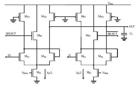
Figure 9. Multiplexer Implementation using Triple-Tail Cell-based PFSCL
The PFSCL and Triple-Tail implementations, both have their own advantages and disadvantages. The PFSCL implementation uses fewer gates, but increased power dissipation while the Triple-Tail based implementation uses a higher number of gates, only if designer sticks to triple tail NOR-based realizations, but helps in reducing the power consumption by approximately 50 percent. Further, Triple- Tail reduces the propagation delay by a mind-boggling 79.24% and the Power-Delay product by 89.6%. Therefore, a hybrid PFSCL topology striking a trade-off between the two implementations is proposed, to obtain even better characteristics. As NOR and NAND gates are readily available in extremely compact designs in conventional PFSCL, the C-Muller design is much more efficient in this implementation as shown in Figure 9. On the other hand, extremely proficient AND gate and D-Latch fundamental cells are available in Triple Tail, making the implementation of DETFF which uses D-latches and multiplexer extremely efficient as shown in Figure 10.
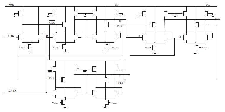
Figure 10. DETFF Implementation using Triple-Tail Cell-based PFSCL
For evaluating the proposed hybrid design as opposed to the conventional PFSCL and Triple-Tail Cell-based PFSCL, a FIFO sequencer has been implemented using 0.18 um CMOS technology. The simulation environment parameters are listed in Table 2. The software, SPICE simulations are performed for all the designs and corresponding waveforms and characteristics are obtained.
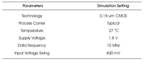
Table 2. Simulation Environment
The obtained waveforms can be validated by checking the functioning of latch and logic circuit. For a given DIN signal and the variations of REQ and ACK signals, the resultant DOUT waveform is obtained as shown in Figure 11. The voltage is varied between 1.4 V (low) to 1.8 V (high) with a 400 mV swing. The REQ and ACK signal both have a frequency of 10 MHZ and both having a duty cycle of 50%. As mentioned in the parameters of the simulation environment, DIN has a frequency of 10 MHz and duty cycle 60% and DOUT is obtained accordingly. The resultant waveforms were analyzed to check the proper functioning of the FIFO sequencer and further to draw the following conclusions:
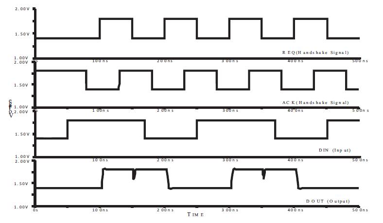
Figure 11. Timing Diagrams and Waveforms for Asynchronous Pipeline
The simulation results are compacted in Tables 3 and 4 via rigorous evaluation of the observations. Various characteristics such as Power Dissipation, Number of transistors, Propagation Delay and the Power-Delay product (PDP) have been used to contrast the upsides and downsides of the three implementations. It is apparently visible that the power dissipation for hybrid topology is reduced by a factor of 37.5% as compared to PFSCL, whereas when compared to Triple-Tail, it reduces by 13.5%. The propagation delay for the hybrid topology improved significantly by a factor of 62.3% and the Power-Delay Product by 84.64% as compared to conventional PFSCL. Further, area overhead has been reduced by 19.5% and 16.4% juxtaposed to PFSCL and Triple-Tail respectively, in the hybrid implementation.
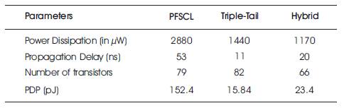
Table 3. Comparison between PFSCL, Triple-Tail and Hybrid Architecture
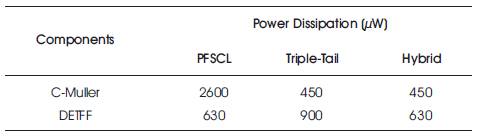
Table 4. Comparison of Power Dissipation for C-Muller Element and DETFF using Specified Topologies
This paper proposes a novel hybrid PFSCL based implementation of FIFO sequencer, a typical asynchronous pipeline. Initially in the paper, PFSCL and Triple-Tail Cellbased implementations have been elucidated, making it easy to discern the latter proposed hybrid topology. Aimed at encapsulating the best parts of both, PFSCL and Triple- Tail, the proposed hybrid implementation strikes a middle ground in terms of the power-delay product and exhibits a considerable reduction in power dissipation and area overhead (characterized by the number of transistors). The proposed topology hence provides the most efficient technique to implement asynchronous circuits using Positive Feedback Source Coupled Logic and its variants.