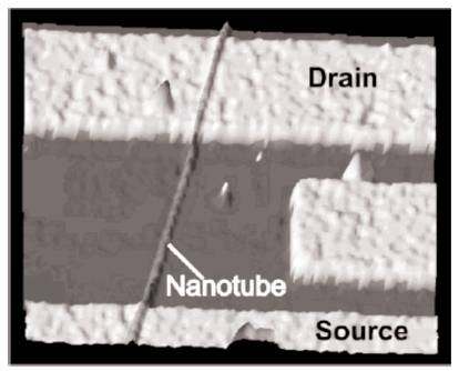
Figure 1. Back-gated CNFET
This paper explores the insights of the most outstanding application of carbon nanotube in electronic field, the carbon nanotube field-effect transistor (CNFET). The motivation of research in CNFET is fuelled by the unique electrical features of CNT, especially the semiconducting feature. Besides, the continuous effort to find future nanoelectronic device that can perform as excellent as MOSFET also push the research of CNFET to be more aggressive. The first section gives an overview of the structure of CNFET followed by the explanation of CNFET operation as a switching device. The next section provides the comparison between CNFET and MOSFET. In this paper, a comparison is being made between conventional MOSFET and different types of CNFETs, and finally concluded a future replacement of MOSFET. The major difference in CNFETs and MOSFET is that it has CNT in channel instead of Silicon. CNFETs show improved characteristics with scaling of technology. CNFET bandgap is directly affected by its chirality and diameter, which is the biggest advantage over MOSFETs. The study of various types of CNFETs comparison has been made in this paper.
The structure of CNFET fundamentally look likes the structure of MOSFET except that the Si channel is replaced by the CNT. Nevertheless, the arrangement keeps changing in order to improve the performance of the device. In this section, the structure of CNFET is discussed. The structure can be categorized as back-gated CNFET, top-gated CNFET, and lately a new structure has been initiated known as vertical CNFET. The progress in silicon technology continues to run on the historic pace of Moore's Law, but the end of device scaling now appears to be only 10 to15 years aside. Therefore, it is of acute interest to search new, molecular-scale devices that might accompaniment a fundamental silicon platform by providing it with new potentials or that might even substitute existing Si technology and permit device scaling to continue to the atomic scale. As the size of device approach the nanoscale, new chances arise from exploiting the physical and chemical properties at the nanoscale. The intrinsic physical properties like density, conductivity and chemical reactivity of bulk materials (example, a copper wire, a cup of water) are independent of their sizes [1-15]. Nanostructures are special as compared with both individual atoms/molecules at the macroscopic bulk materials and at a smaller scale. They are known as mesoscopic structures. Research of Nanoscience focuses on the extraordinary properties of nano range structures and materials which does not exist (or exist only very weakly) in structures of identical material composition, but at other scale ranges. Molecular Electronics with Carbon Nanotube are the future of electronic circuits [17-27]. Initially, Carbon Nanotube Field-Effect Transistors were simple devices manufactured by depositing single-wall CNTs (synthesized via laser ablation) from solution onto oxidized Si wafers which had been pre-patterned with gold or platinum electrodes. The electrodes performed as source and drain, connected through the nanotube channel, and the doped Si substrate served as the gate. But now several other techniques are being investigated for fabrication of CNFET. Gas-phase catalytic growth of SWNTs from carbon monoxide is crucial for CNTs [29-32].
Tans et al. [28] for the first time demonstrated CNFET in 1998 to show a technologically exploitable switching behaviour and marks the inception of CNFET research progress. They managed to modulate the conductivity more than five orders of magnitude by applying electrical field to the nanotubes [24]. Most of the earlier CNFET devices were back-gated with very thick gate insulators made of silicon oxide approximately around 100 nm-150 nm [16]. The structure used a non-local back-gate with the carbon nanotube side bonded to noble metal electrodes [33] . A type of metal that resists the attack of acids and other reagents, does not corrode as well as it is called as Noble metal. The picture of back-gated CNFET and the schematic cross section of back-gated CNFET are given in Figures 1 and 2 respectively.
Figure 1. Back-gated CNFET
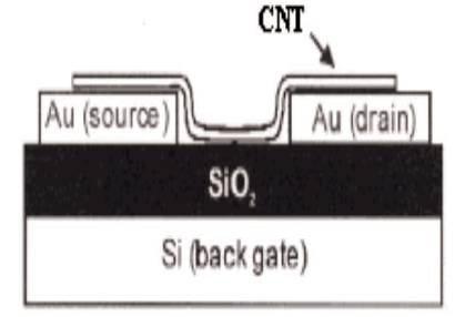
Figure 2. Schematic Cross Section of Back-gated CNFET
This premature formation results in poor attributes like small drive current, low transconductance (10-9 S) and large contact resistances (>1MΩ) [26]. Since the carbon nanotube is just simply laid on the gold electrode, the bad contacts and weak van der Waals force leads to the unsatisfactory characteristics [16]. The performance can be improved by increasing the gate capacitance by decreasing the insulator thickness or extending the dielectric constant. Though, the gate capacitance calculation of CNFET is different from MOSFET. The commencement of Al2O3 layer on top of patterned Al gate is capable to lesser the gate voltage and rises the transconductance [24]. Moreover, enhancement is followed by the inauguration of top-gated structure. In order to have a complex integrated circuit, each CNFET needs to be gated individually.
The next generation of CNFET came in top-gated structure, which enhanced the device performance. This new structure is expected to bring better results, since the performance of back-gated structure is quite poor in terms of the device operation. Also this structure is fabricated by dispersing the carbon nanotube on an oxidised wafer [16]. Atomic Force Microscopy (AFM) picture is used to recognize the single carbon nanotube and then the source and drain terminals, which made of Ti, are fabricated on top of CNT. A gate dielectric film about 15 nm-20 nm is deposited at 300 °C through Chemical Vapour Deposition (CVD) process. Finally, using lithography a 50- nm-thick gate electrode is patterned. Figure 3, represents the structure of top-gated CNFET.
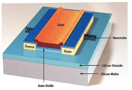
Figure 3. Top-gated Structure of CNFET
This structure offers better out-turn than the prior structure. The advancement comes from the scaling of the dimension and the acquisition of better device geometry as well as the device performance[33]. For instance, the electrical field is expanded because of the device geometry and contact resistance is lessened by picking an appropriate contact material. Furthermore, the threshold voltage is altogether lower than the back gated structure, and drive current is much higher and transconductance is comparatively high (3.35μS for every nanotube).
Vertical CNFET is the latest development that has been reported in field of CNFET progress. Choi et al. [34] proposed the structure with surround-gated in 2004. The size of the transistor can be as little as the diameter of CNT which fits to tera-level CNFET and density of 1012 elements per cm2 . The developing of vertical CNFET includes the forthcoming strides: nano-pore arrangement by anodization took after by synthesizing the carbon nanotube, metalelectrode development, oxide deposition and designing and lastly gate electrode development. SiO2 is deposited at the top of aligned CNT by electron gun evaporation, chased by holes formation of e-beam patterning and chemical etching. Deposition of top gate electrode follows the silicon oxide deposition process. The structure of vertical CNFET is given in Figure 4.
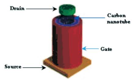
Figure 4. Device Structure of Vertical CNFET
In the above structure, every carbon nanotube is electrically joined to the bottom electrode, source, upper electrode (drain), and gate electrode is put around the carbon nanotube. Every cross point of source and drain electrode compares to a transistor component with a solitary vertical carbon nanotube. The hole-diameter of gate oxide decides the number of carbon nanotubes in the transistor. The vertical CNFET permits higher packing densities that can be attained since source and drain areas can be organized on top of each other [24]. On the other way, since the active devices are no longer bound to the surface of mono-crystalline silicon wafer, real 3-D structures can be build possible. The other view of vertical CNFET is shown in Figure 5.

Figure 5. Another view of Vertical CNFET
The fundamental guideline operation of CNFET and MOSFET continues as before, where electrons are given by source terminal and drain terminal will gather these electrons. As it were present is truly flowing out of drain to source terminal. The gate terminal will control current intensity in the transistor channel. The transistor stays off state, if no gate voltage is connected. In the accompanying segment, the operation of two distinct structures is talked about. The underlying structure is called Schottky-Boundary CNFET and the later one is MOSFET-like CNFET. The contrast in the structures of these two CNFETs is somewhat distinctive, however it brings about various transistor operation.
Schottky Barrier (SB) is a potential barrier that exists at every contact between metal and semiconductor. The barrier's height is decided by filling of the metal-induced gap states. The metal-induced gap states become available in the energy gap of semiconductor caused by the interface made with the metal. The SB is controlled by the local work functions distinction of the metal and CNT. Schottky Barrier is additionally colossally delicate to the changes of local environment at the contact [35]. Case in point, the gas adsorption differs the work function of metal surfaces. In perspective of the way, that this device utilizes metal as its source/drain terminals and Schottky Barrier at its terminal contact between CNT and metal, and so it is known as SB Carbon Nanotube Field Effect Transistor. The diagrammatic view of SB-CNFET is given in Figure 6.
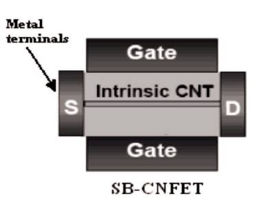
Figure 6. Schottky-Barrier CNFET (SB-CNFET)
Direct tunnelling through the Schottky barrier at the sourcechannel junction forms the principle of SB-CNTEFT. The gate voltage controls the barrier width and hence the device transconductance depends on the gate voltage. In the channel, enormous barrier limits the current at short gate bias. If the gate bias is increased, the barrier width is lowered, which in turn increases quantum mechanical tunnelling through the barrier, hence an increased amount of current flow in transistor channel. By regulating the transmission coefficient of the device, the transistor action occurs in SB-CNFET.
SB-CNFET manifests very robust ambipolar conduction, particularly when the gate oxide thickness is diminished, even the Schottky Barrier is zero [36]. This kind of conduction causes leakage current to rise exponentially with supply voltage, especially when the nanotube diameter is large, which results in limiting device potential. Therefore, in order to improve the performance of SB-CNTFET, the ambipolar conduction must be reduced. In this direction, one of the solutions is to increase the gate oxide thickness. If the thickness of gate oxide is excessive, no ambipolar conduction exists when Schottky Barrier is zero. The leakage current is, thus, reduced and as a result, the transistor performance is improved. Another alternative is to build asymmetric gate oxide, proposed recently to suppress the ambipolar conduction [37].
Another issue with SB-CNFETs is that they suffer from metalinduced- gap states, which limits minimum channel length and thus increases the source to drain tunnelling. SB-CNFET is also incompetent to place gate terminal close to source because it can increase the parasitic capacitance.
MOSFET-like CNFET have structures slightly different than Schottky Barrier-carbon nanotube field effect transistor, since they use heavily doped terminals instead of metals. In order to overcome the problems encountered in SBCNFET, these are operated like normal MOSFETs. Dissimilar SB-CNFET, source and drain terminals are heavily doped like MOSFET and hence called as MOSFET-like CNFET. The device as shown in Figure 7 works on the principle of modulating the barrier height by gate voltage application. Here, the drain current is controlled by a number of charges, that is induced in the channel by the gate terminal.
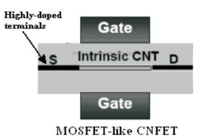
Figure 7. MOSFET-like CNFET
These have the following advantages over SB-CNFET.
CNFET are regularly p-type, which implies they are adjusting current in the channel when negative gate voltage is connected to the device. For p-type operation, when negative gate voltage is connected, it will lead current in the channel from source to drain and this current is because of the movement of holes. Conversely, an n-type CNFET conducts at whatever point a positive gate voltage is connected to the device, which is the current stream in the channel from source to drain is because of the conduction of electrons. To put it plainly, CNFET conveys current when either a positive or negative gate voltage is connected. This characteristic, permitting both holes and electrons conduction in the same device, is called ambipolar characteristic. Along these lines, CNFET is an ambipolar device, since it conducts current either in negative or positive supply voltage.
Normally, when CNT is utilized to create CNFET with no further preparing, the devices are invariably p-type. Therefore, with a specific-end goal to deliver n-type CNFET, another process is required. There are two methods for creating n-type CNFET from p-type CNFET. The transformation process can be made possible either annealing or doping process.
Annealing is a procedure of changing over p-type CNFET into n-type CNFET through vacuum annealing. In this process, p-type CNFET is warmed under vacuum to desorb any adsorbed gas, for example, oxygen and toward the end of this process, the p-type CNFET is changed over into n-type CNFET. This conversion process is reversible on the grounds that if n-type CNFET is exposed to air, the device will come back to its original p-type characteristic. The way toward annealing is graphically appeared in Figure 8.
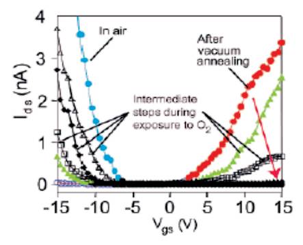
Figure 8. Characteristic of CNFET due to Annealing Process
Another process is in which the p-type CNFET is doped utilizing electron donors, for example, alkali metals and is portrayed in Figure 9. This is called doping process, Alkali metals, for example, potassium, will give the same result as in annealing process with p-type CNFET is changed into ntype CNFET. Conversion process from p-type to n-type and vice versa is imperative particularly to create nanotube complementary logic circuits. Along these lines, this transformation gives a potiential solution to assemble nanotube-based logic circuit following for building complimentary logic circuits both p-type and n-type CNFET are required.
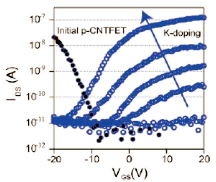
Figure 9. CNFET Characteristic due to Exposure to Potassium Atom
In this segment, the authors have given a brief comparison between the performance of CNFET and MOSFET.
The variation of drain Current (Id ) vs drain voltage (Vd ) at 0.1 nm diameter, 0.2 nm diameter and 1 nm diameter are shown in Figures 10, 11, 12 respectively. CNFET bandgap is directly affected by its chirality and diameter, which is the biggest advantage over MOSFETs. The study of various types of CNFETs comparison is made in this paper.
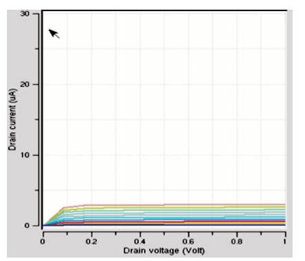
Figure 10. Drain Current (Id) vs Drain Voltage (Vd) at 0.1nm Diameter
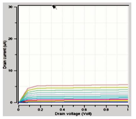
Figure 11. Drain Current (Id) vs Drain Voltage( Vd) at 0.2nm Diameter

Figure 12. Drain Current (Id ) vs Gate Voltage (Vg ) at 1nm Diameter
Table 1 shows that the energy band gap of the CNT is inversely proportional to the nanotube diameter (Egap  1/Diameter)
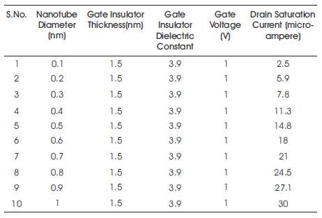
Table 1. Energy Band Gap of CNT and Nanotube Diameter
MOSFET has been used widely in electronics industries. With the increasing technology, the authors are scaling down the channel length of MOS, which may result in many short channel effects. To get rid of all these drawbacks of conventional MOSFETs, the authors are studying the CNFET (Carbon Nanotube Field Effect Transistors). In this paper, a comparison is being made between conventional MOSFET and different types of CNFETs. And finally concluded a future replacement of MOSFET. The major difference in CNFETs and MOSFET is that, it has CNT in channel instead of Silicon. CNFETs show improved characteristics with scaling of technology.
In this paper, several basic principles of CNFET are explained. Starting with various types of CNFET structure, followed by the operations of CNFET. From this paper, it can be seen that from CNFET structure and its behavior, this device is actually more or less as same as MOSFET except that the material for transistor. Besides, Carbon Nanotube Field Effect Transistor will play important role in designing of electronic circuits which are the base of digital computers.