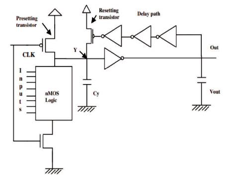
Figure 1. SRL Technique
This paper presents a new optimized technique to power reduction and performance improvement based on selfresetting logic. The concept of self-resetting logic uses the concept of resetting the output logic automatically after a certain time span. The proposed circuit eliminates the problems of SRLGDI logic proposed previously. SRLGDI was proven to be better than dynamic logic, CMOS self-resetting logic and GDI. Three designs of full adders were made using SRLGDI and a final proposed design was made using modified SRLGDI logic and compared to three SRLGDI designs to prove the performance improvement achieved using the modified SRLGDI logic.
With advancement in low power portable electronic device space, there is an increase in requirement of low power circuit techniques and standard cells. These low power portable devices include communication devices, multimedia, handheld measurement equipment and processing units.
Over the years, many low power techniques have been proposed which have been proved to be superior to conventional CMOS logic in terms of power consumption, delay performance or area overhead. Some of the techniques include pass transistor logic, GDI logic, adiabatic logic, and dynamic logics [17] like NORA CMOS, domino logic, etc. These techniques provide benefits over CMOS in aspects and fall back in other aspects [4,5]. As pass transistor logic and GDI logic are better in terms of power and the number of devices required to implement particular logic in comparison to CMOS [13], at the same time these two techniques have drawbacks like logic level drop of V . Problems in these techniques were addressed in t Complementary Pass Transistor Logic (CPL) [10], and Swing Restored Pass Transistor Logic (SRPL). Similarly, dynamic logic circuits are better in terms of propagation delay, and power consumption, but the drawbacks include problems like charge sharing, synchronization, etc. Different techniques have been proposed by different authors to handle issues observed in dynamic logic circuits. Some of these techniques include feed through logic and Self Resetting Logic (SRL) [16].
Some techniques to take advantage of high speed of dynamic logic and efficient logic implementation of pass transistor and GDI logic have also been found. These techniques use a mixed approach to address the problems observed in circuits when designed with single technique alone. One such technique is self-resetting logic with GDI. This work draws motivation from this technique and uses this study as a base for the proposed technique as described in remaining sections of the paper.
SRLGDI technique [2] uses a mixed approach, where Self Resetting Logic (SRL) has been used as a base and the logic evaluation circuit as used in SRL has been replaced by Gate Diffusion Input (GDI) logic [1] to take advantage of low transistor count in logic evaluation circuit. The rest of the paper is divided into three sections, i.e. concept and problem statement, proposed technique, results and conclusion. Section 2 is the concept section that covers the base theory and related concepts which are essential and have been utilized in base design/proposed design. Section 3 presents the details of proposed design and its function. In section 4, the results of power consumption, delay, and PDP are presented and compared with SRLGDI technique by taking full adder as a design for reference.
The scaling of technology and power consumption by VLSI circuits have always been a major concern for the ASIC designers to which different approaches have been applied to overcome the problem of power and delay. The main objective of this work is to design power efficient high speed adders using Self Resetting Logic.
As discussed in previous section, Self-Resetting Logic is the base of SRLGDI. The concept of SRL is shown in Figure 1. It shows the preset / evaluation circuitry which charges the node V through PMOS in preset phase. NMOS at the foot is active while evaluation and provides a discharging path to node V through NMOS logic network. NMOS logic network is the logic evaluation part of the circuit which determines the logic behavior of the circuit. The delay chain consisting of three inverters drive the resetting PMOS transistor [12] parallel to PMOS device of preset / evaluation circuit. In order to optimize SRL technique [15,16], the SRLGDI technique replaces the NMOS logic block present in SRL by logic block implemented using pure GDI logic. Gate Diffusion Input (GDI) technique as given in [3] uses standard cell having four ports, out of which three are used as inputs and one as output.
Figure 1. SRL Technique
Use of this standard cell helps in achieving transistor count as less as four in implementation of two input XOR gates, which takes eight transistors using CMOS logic when complemented inputs are provided. The basic schematic showing SRLGDI [14] logic is presented in Figure 2.
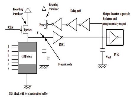
Figure 2. SRLGDI Technique
The technique uses only preset and reset [7,8] transistor and there is no tail NMOS transistor. This results in always active GDI logic block which consumes power as well as it causes contention in case when the output of the circuit is low and the reset transistor turns on to pull it high. This case results in even more current consumption [6].
The identified drawbacks of the design are always active GDI block and the case of contention between output and reset PMOS.
The design proposed in this work addresses the issue identified in SRLGDI design. The issues discussed above have been addressed in the proposed design (Figure 3) by turning off the supply of GDI block [8,9], and all inverters in delay chain during preset phase. The clock polarity for preset and evaluation phase has been reversed and the number of buffers used has been optimized according to logic to avoid the case of contention.
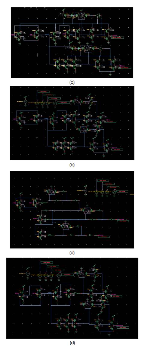
Figure 3 (a) Proposed Full Adder using Modified SRLGDI Technique, (b) Full Adder-1using SRLGDI [2], (c) Full Adder-2 using SRLGDI [2], (d) Full Adder-3 using SRLGDI [2]
A set of PMOS and NMOS is used to control power of GDI block and inverters. When clock = logic 1, the output is set to low through reset NMOS and all inverters and GDI logic has a Vdd =0. When clock = logic 0, the GDI blocks and inverters receive proper supply and evaluate output according to the inputs available. The proposed design is shown in Figure 4. The designs presented in [2] are shown in figures below.
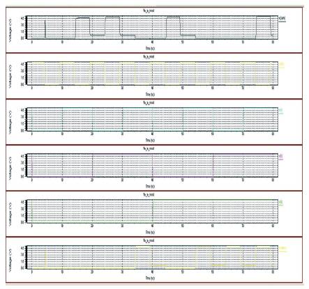
Figure 4. Waveforms of the Proposed Full Adder using Modified SRLGDI
The proposed design is working as expected with the proposed logic evaluation and logic values. Figure 4 shows that the design has a better power and delay performance in comparison to the design in [2].
Three designs of full adders using SRLGDI [2] and same design of full adder by applying modified SRLGDI technique were made to compare performance of the techniques (Table 1). The results obtained from SPICE simulations of the designs are shown below.
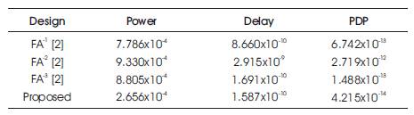
Table 1. Performance Summary and Comparison
A new technique based on GDI SRL was proposed with the advantage of low power consumption to the existing technique [11]. The proposed technique shows two- fold improvement in power consumption and considerable improvement in delay of the sum and carries outputs. The proposed design can be used in low power logic circuits due to its low power and device count. Further work can be done on the improvement of logic levels and of the design and optimization in terms of the number of devices. The proposed technique can also be modified to be used with other dynamic logic circuits which use input resetting in precharge phase.