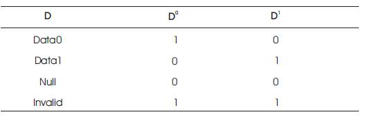
Table 1. Dual Rail Encoding
An adder is a device, that adds two numbers and generates the summed result. In digital circuits, there are so many adders like carry select adder, ripple carry adder, carry skip adder, ling adder, manchester carry-chain adder and so on. Among all adders, parallel prefix adder is a highly-efficient binary adder. These parallel prefix adders are implemented in a new topology called Static Null Conventional Logic (NCL) gates. NCL gates are asynchronous circuits which are independent of the clock skew problem, delay and consumes less power. The static implementation of conventional versions of NCL gates use a set of extra minimum-sized transistors to cut off connections to the power rails in specific nodes while the gate is switching. Implementation of parallel prefix in NCL gates, increase the area overhead problems that occur, but the power consumption reduces due to connecting and disconnecting of the specified gate terminal.
As we know, synchronous circuits have many disadvantages like the clock skew problem, sensitive to variation in physical parameters, no module reusability, and more power consumption [1]. These disadvantages are overcome by asynchronous circuits and mainly the clock skew problem is eliminated because, they are clock-less devices. In asynchronous circuits, event sequencing and control depends on local handshake protocols rather than on a global clock signal [2]. Here, quasi-delay insensitive (QDI) circuits are used; these circuits are correct-by-construction that uses multi-rail signals. It gives an average case performance rather than a worse case performance [3]. Quasi-delay circuits are glitch free circuits and can be easily interfaced with multi-rated circuits.
An adder plays a vital role in digital signal processing systems. Parallel Prefix Adder is a high speed adder with regular fan-out. The main objective of parallel prefix adder using static conventional logic gates is to reduce the power consumption, delay and to increase the speed. Though the area overhead problem occurs by using static NCL gates, power consumption can be reduced by simply disconnecting the power rail between the gate terminal and the supply voltage.
Asynchronous techniques such as, Null Convention Logic (NCL) have many advantages due to the elimination of global clock and here the timing analysis is not necessary for the correct operation. Dual-rail signal encoding is more popular, and it is similar to the traditional boolean logic. Assuming isochronic wire forks [6], they must meet the input-completeness and observability criteria [4]. Table 1 shows the dual-rail signal encoding. A dual rail signal, D, consists of two wires, D0 and D1 . If D0is one, then only DATA0 will assert. If D1 is one, then only DATA1 will assert. If both D0 and D1 are zero then NULL is asserted. If both D0 and D1 are one, then it is coded as INVALID [5]. Using the dual rail encoding within less time (less delay), the output will be obtained.
Table 1. Dual Rail Encoding
The basic component of a NCL gate is threshold gate. The primary type of threshold gate shown in Figure 1 is the THmn gate, where 1 ≤ m ≤ n. THmn gates have n inputs. Atleast m of the n inputs must be satisfied to assert the output. In a THmn gate, each of the n inputs is connected to the oval shape of the gate, the output is given out of the pointed end of the gate and the gate's threshold value, m, is written inside of the gate. It represents the threshold value [9], [8], [13].
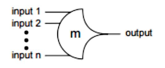
Figure 1. THmn Threshold Gate
Another type of threshold gate is the weighted threshold gate, denoted as THmnW w1 w2 …wR . Weighted threshold gates have an integer value, m ≥ wR > 1, applied to input R. Here 1 ≤ R < n, where n is the number of inputs, m is the gate's threshold and w1 , w2 , …wR , each > 1, are the integer weights of input1, input2, … inputR, respectively. For example, consider the TH34W2 gate, whose n = 4 inputs are labeled A, B, C, and D, as shown in Figure 2 [10], [13].
Figure 2. TH34w2 Threshold Gate
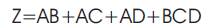
Input A has the weight of value 2 and other inputs B, C and D have weights of value 1. To get the output Z, input A must be asserted along with any other inputs B, C, or D. NCL threshold gates are designed with hysteresis state-holding capability, such that after the output is asserted, all inputs must be deserted before the output will be deserted [10] NCL circuits are comprised of 27 fundamental gates as shown in Table 2 [13].
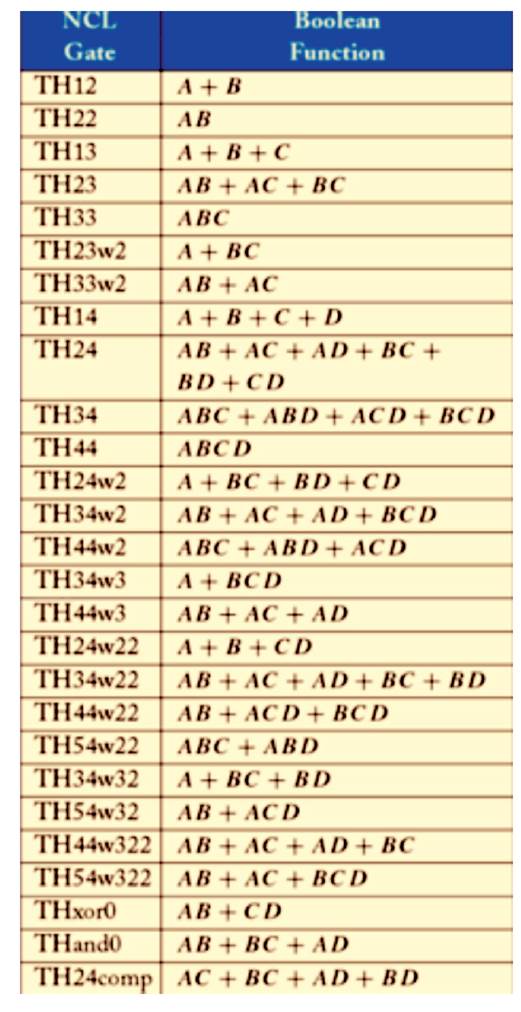
Table 2. 27 NCL Fundamental Gates
Semi-static implementation of NCL gates uses weak feedback. Due to the presence of weak feedback inverter, current leakage takes place at node Y. Due to this leakage, the supply voltage gradually decreases and becomes zero. This semi-static gate does not support quasi-delay circuit completely due to the absence of hysteresis mechanism. The charge sharing problem that occur in semi-static gates is overcome by static NCL gates. Semistatic architecture is shown in Figure 3. Here SET block is built in nmos transistors and RESET block is built in pmos transistor. TH23 semi-static NCL gate are implemented as shown in Figure 4.
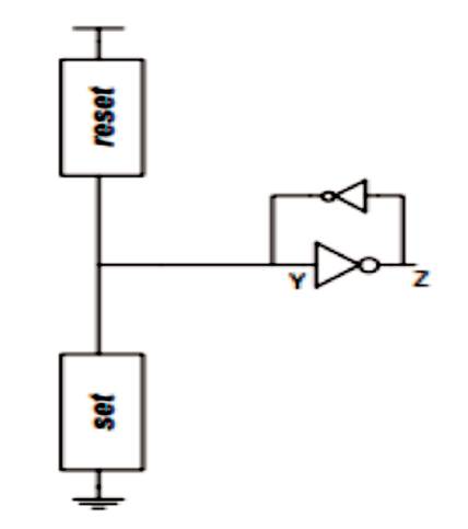
Figure 3. Structure of a Semi-static NCL Gate
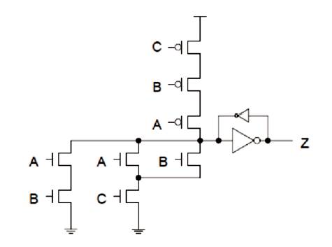
Figure 4. Semi-static Implementation of a TH23 Gate
The TH23 gate is realized in the semi-static structure SET block is replaced by TH23 of boolean function and RESET block is replaced by a series of pmos transistors. If AB or BC or AC are logic 1, then the output is asserted to logic 1.
Once the output becomes asserted, it remains asserted until all the inputs are de-asserted [7]. The RESET block will be ORing all the inputs because the main aim of ORing input gates is to reduce transistor count as much as possible.
To overcome the problem of leakage, and charge sharing effect, the authors opt for a static NCL gate. Implementation of static NCL gate is shown in Figures 5 and 6.
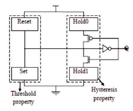
Figure 5. Static NCL Topology
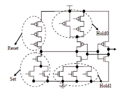
Figure 6. TH33W2 NCL Gate
This implementation additionally has pull-up and pull-down networks called Hold0 and Hold1 to store the state information which is impossible in semi-static NCL gates due to the presence of weak feedback inverters. The SET from Figure 5 represents the boolean functionality of the gate, RESET corresponds to ORing all the inputs together while Hold0 is the complement of a set, i.e Hold0=set, and Hold1 is the complement of reset, i.e Hold1=reset [7].
Figure 6 shows the static implementation of TH33w2 NCL gate where n=3 and m=3. If either AB or AC is asserted, then the output is asserted, it remains same until all the inputs are set to zero.
Figure 6. TH33W2 NCL Gate
The parallel prefix adder is a Kogge Stone adder form a carry look ahead adder. It generates the carry signals in O(log n) time, and is widely considered as the fastest adder design possible. It is the common design for highperformance adders in industry. It takes more area to implement, but has a lower fan-out at each stage, which increases the performance. Wiring congestion is often a problem for parallel prefix adders as well. Parallel prefix adder [9] is implemented in static NCL gates. It is one of the high-speed adders with less delay and high speed. Their total delay, average power and performance (speed) are calculated [1]
This red, yellow and green block are implemented in static NCL gates, XOR gate can be implemented using THxor0 AND and OR gates are replaced by TH12, TH22 static gates respectively using the boolean function as shown in Figure 7 [11].
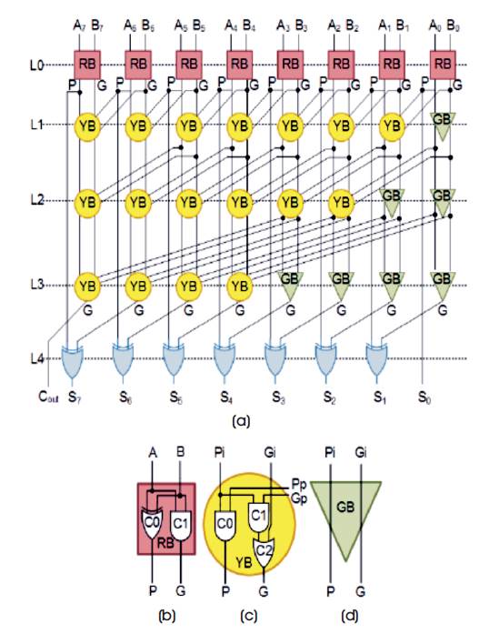
Figure 7 (a) Parallel Prefix Adder (b), (c), (d) Individual Blocks of a Parallel Prefix Adder
The adders to be studied were designed with static NCL gates. Source code is written in SPICE language. The hspice-a_2008.03 tool is used to simulate the program, and awanwaves are used for visualizing the output waveform. 180nm technology is used for pmos and nmos transistors. Measure statement is used to calculate the Total Delay (TD) and average power. Total delay is known as the time taken for a signal to travel from input to output. The delay is inversely proportional to speed, and by simply inverting the delay parameter, we get the speed parameter. Though area is huge, the power consumption is less because the supply voltage is turned off between the gate terminal and power rail hence, unused transistors will simply turn off, or turn on when conduction is needed.
Results of red block is shown in Figure 8. It is already known that, the NCL gate uses dual rail encoding for every bit that has two wires to transmit data i.e DATA0 and DATA1. Red block inputs are A and B. If input is one, then A_1 and B_1 wires will assert, and if input is zero, A_0 and B_0 wires will assert. In simulation results, A_1 is asserted and B_0 is asserted, then the truth table of EX-OR gate, AND gate results in the output of P as one (It is clearly shown in Figure 8, green line increases as time increases) and output of G as zero.
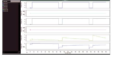
Figure 8. Output Waveform of Red Block
Simulation results of yellow block are realized as shown in Figure 9. Here 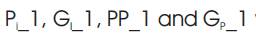 wires are asserted and the outputs of P and G is one (It is clearly shown in Figure 9, outputs are increasing with time). In green block, whatever the value available in P and G, the same value i i will propagate to P and G. For a 8-bit parallel prefix adder, cin =1, here the 8-bit input sequence is A0 =0, A1 =0, A2 =0, A3=0 A4 =1, A5 =1, A6 =1, A7 =1 and the 8-bit input sequence is B0 =1, B1 =1, B2 =1, B3=1, B4 =0, B5 =0, B6 =0, B7 =0. The output of adder is S0 = 1, S1 = 1, S2 = 1, S3 =1, S4 =1, S5 =1, S6 =1, S7=1 and the output of carry, c0 =0. Simulation results are shown in Figure 10. The main reason why asynchronous circuits are not in high demand is the lack of CAD tools. Parameters are tabulated in Table 3.
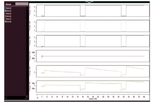
Figure 9. Output Waveform of Yellow Block
Figure 10. Output Waveform of Parallel Prefix Adder
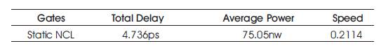
Table 3. Total Delay, Average Power and Speed of Parallel Prefix Adder in NCL Gates
The proposed adder is faster because of less delay compared to other basic adders. An efficient parallel prefix adder is designed using NCL topologies to achieve better speed performance with less delay. It is noticed that Kogge-Stone adder performs speed calculations with less power consumption. If the area of adder increases, the cost increases, since it requires more wires for connection. The calculation of path delay is based on timing analysis, but here delay insensitive circuits like NCL gates are used. If area increases, there will be no major delay in the circuit. NCL gates are reliable gates that the power consumption will be reduced, and speed will be increased due to the elimination of global clocking, which gives an average case performance.
As an ongoing work, the authors are designing differential gates for NCL+ [12]., which are another recently proposed family of NCL gates. Having these gates will then enable to explore the automation of the synthesis of NCL circuits.