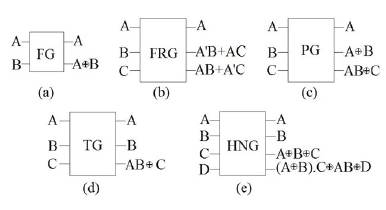
Figure 1. Structure of (a) Feynman (b) Fredkin (c) Peres (d) Toffoli and (e) HNG gate
In CMOS logic, there is a steady increase in power dissipation which appears in the form of heat to the surrounding environment and affects the reliability. The research efforts are made towards looking into alternatives that go beyond the traditional CMOS technologies, and reversible logic has emerged as a promising choice. In this paper, an optimized and cost efficient realization of reversible Braun multiplier is presented. The design of a 4x4 bit multiplier is developed, designed and presented in this paper as an illustration. The architecture is iterative and hence this can easily be extended to the generalized multiplier of any order. The proposed design of a 4x4 reversible Braun multiplier uses three types of reversible gates namely, PG, HNG and TG gates. The proposed design is compared with an already presented reversible multiplier design showing that the proposed multiplier design is more efficient in terms of quantum cost, constant inputs, garbage outputs and the number of elementary reversible gates
The CMOS technology has constantly moved to take up a central position in electronic system design. It finds the use in most of the cutting edge commercial applications. The processes have shrunk and the design automation tools are in common place. This has accelerated the design of complex chips operating at higher frequencies than a decade ago. Although, the basic CMOS design principle remains unaltered, there is a significant change in the emphasis and approach of the design. There is a steady increase in power dissipation in the form of heat to the surrounding environment which affects the reliability. The research efforts are made toward looking into alternatives that go beyond the traditional CMOS technologies and reversible logic wherein operations performed in an invertible manner have emerged as a promising choice. New technologies are introduced to reduce heat generation but Landauer (Landauer, 1961) pointed out that, the gates always dissipate energy regardless of underlying technology. There is loss of information in classical computing, which is a dissipative process. The entropy of system is reduced by ΔS = κ ln2 for every bit of information that is lost during computation process, and hence H = TΔS = κT ln2 Joules of heat is dissipated where κ and T are Boltzmann's constant and absolute temperature respectively. In 1973, Bennett (Bennett, 1973) of IBM research showed that, a classical computing can be broken down into a series of steps which can be performed reversibly, it is emphasized that, a reversible computer can run forward till the completion of computation to get the final result, print the result, and then reverse back all of its steps to return to its initial step and thus resulting in no heat generation. The literature survey on reversible logic shows that a progress has been made in the direction of exploring new reversible gates and applying the concepts to the areas such as DNA computing (Sarker, 2011), cellular automata (Morita, 2008), cryptography and encoding/ decoding methods (McGregor, John Patrick & Lee, 2001).
Multiplication is an essential operation used in almost all the modern digital systems including digital signal processors, bioinformatics, complex image processing and microcontrollers. The performance of the digital system depends heavily on the multiplier due to its extensive use. It is therefore, highly desirable that, these are fast and consume low power without performance degradation. In an effort to apply reversible logic to multiplier, the objective of this paper is to address design of reversible Braun multiplier. The paper is organized as follows: Section 1 presents the background on reversible gates followed by Section 2 which briefly reviews related work. The proposed design is presented in the Section 3. The results and discussions are included in Section 4. Then, Section 5 is comparison. Finally the paper is concluded.
A reversible function always have an equal number of input and output lines, with each of the input-output combinations being unique. Therefore, there is a one-to - one correspondence between input and output of any reversible circuit. A non-reversible boolean function can always be implemented by a reversible circuit after appropriately transforming it to a reversible logic with the help of reversible gates by adding ancillary input bits, and garbage bits. The inputs which assume value '0' or '1' during the operation are termed as constant inputs.
A reversible gate is defined as a block which operates on multiple input lines and produce the desired output logic reversibly. A reversible gate with n input bits and n output bits is represented as an n x n gate. Some of the most widely and commonly used reversible gates (Thapliyal & Ranganathan, 2010) are Feynman (FG), Fredkin (FRG), Peres (PG), Toffoli (TG) and HNG gate. From Figure 1, it may be noted that FG is a 2x2 gate. FRG, TG and PG belong to 3x3 gates and HNG is a 4x4 gate.
Figure 1. Structure of (a) Feynman (b) Fredkin (c) Peres (d) Toffoli and (e) HNG gate
The most important design parameters for any reversible circuit includes its quantum cost, number of constant inputs, number of garbage outputs and the total number of reversible gates used in synthesizing the required logic functionality.
The design of any reversible gate is primarily assessed by these parameters. Smaller these parametric values, the better is the overall design of reversible system. Thus, researchers aim at reducing the total cost, which is the sum of all the parameters as minimum while keeping the system functionality intact.
The quantum cost of a reversible circuit is defined as the number of 1x1 and 2x2 reversible gates required to design the desired Boolean logical function. The quantum cost of reversible gates presented in Figure 1 is listed in the Table 1.
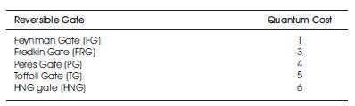
Table 1. Quantum Cost of Common Reversible Gates
Constant inputs are the extra inputs whose value does not change during the entire operation. Their value is fixed to either 1 or 0. They are solely added to make the design reversible.
Garbage outputs of a reversible gate refers to those outputs lines that are not used in further computation as these do not provide any practical functionality to reversible circuits.
Numerous designs of multipliers have been reported in literature till date. High speed low power irreversible multiplier architecture was first proposed by Maaz et al. (Maaz, Abu-Shama, & Bayoumi, 1996). Subsequently various reversible multiplier circuits are reported in the literature. These implementations use existing reversible gates or present a new reversible gate and use it for multiplier design. Reversible multiplier by Zhou et al. (Zhou, Shi, & Wang, 2011) belongs to the second category and presents a new 4x4 reversible gate ('ZS' series gate) for signed multiplication. Many reversible multipliers employ already existing reversible gates. Thapaliyal and Srinivas (Thapaliyal & Srinivas, 2006) have proposed reversible multiplier using TSG gates. Moallem and Ehsanpour (Moallem & Ehsanpour, 2013) developed a 4x4 reversible multiplier which was based on an advanced Partial Product Generation Circuits (PPGC) with peres gates and an optimized peres full adder reversible gate based Reversible Parallel Adder (RPA) part. Shams et al., Haghparast et al. and Haghparast et al. proposed reversible multipliers with two independent modules, one for partial product generation and the other for addition of partial products based on MKG (Shams et al., 2008) and HNG (Haghparast et al., 2008) gates. Similar designs were proposed by Islam et al. (Islam, Rahman, Begum & Hafiz, 2009) wherein, PFAG gate is employed for synthesis. Reversible multipliers using vedic multiplication algorithms have also been recently reported in literature (Saligram & Rakshith, 2013). Moghadam and Navi (Moghadam & Navi, 2012) proposed reversible multiplier design using partial product generation and addition sub-circuit. Two different designs for partial product generation are reported in (Moghadam and Navi, 2012). Design 1 uses an array of PG gates, while design 2 employs an array of TG gates. An additional fan out generation sub circuit was cascaded with design 1. The fan out generation sub-circuit requires four BVF gates to generate four copies for each input bit of Y therefore two identical signals at input are needed. Consequently, the same fan out problem persists and an additional FG gate is required with each of the four BVF gate in order to synthesize a valid fan out generation sub circuit. Therefore, quantum cost, constant input and total number of gate will all be an increment by four. In the design parameters of design 2, the cost of three PG and FG gates is not accounted for.
A brief discussion on conventional Braun multiplier is given first which is followed by proposed design of reversible Braun multiplier. A comparison with existing reversible multiplier is also included.
The conventional multiplication requires series of repeated addition operation where multiplicand (Y) is multiplied by multiplier (X) and results in product (P). The multiplication process is illustrated in Figure 2 for two 4-bit binary numbers. The hardware realization of conventional multipliers require registers having shift capability to store partial products through AND gates and adders to add partial product.
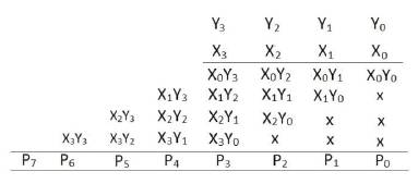
Figure 2. Multiplication of Two 4-Bit Binary Numbers
The conventional Braun multiplier (Figure 3) on the other hand is a parallel array multiplier, where AND gates and adders are arranged in an iterative structure. These multipliers do not require registers to store partial products. In general, a nxn Braun multiplier requires n*(n-1) adders and n2 AND gates. A 4x4 Braun multiplier is depicted in Figure 3, which uses 12 adders and 16 AND gates. The AND gate generate partial products XiYj (i=0, 1, 2, 3 and j=0, 1, 2, 3), and are arranged in four horizontal rows marked as Level 1, Level 2, Level 4 and Level 6. The adders add the partial products and are arranged in four rows marked as Level 3, Level 5, Level 7 and Level 8. The final product is obtained through subsequent stages of adder, as it moves from top to bottom starting from least significant bit of product Po through P7 . A careful inspection of Figure 3 suggests that, FA1 , FA2 , FA3 and FA12 are used to add only two bits, therefore these can be replaced by half adders to reduce overall cost.
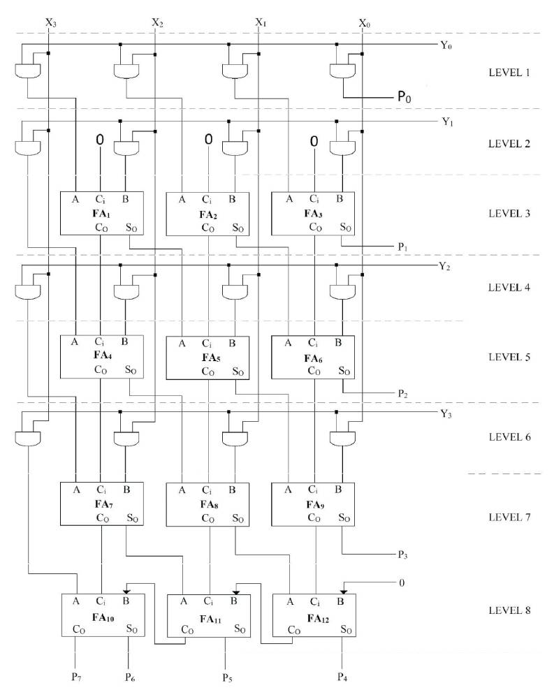
Figure 3. Conventional 4-Bit Braun Multiplier Design
The design of the proposed 4x4 reversible Braun multiplier is described in this section. It uses three types of reversible gates namely PG, TG and HNG gates. The requisite AND gate functionality may be achieved by configuring PG or TG gates as shown in Figure 4(a). The reversible PG and HNG gates are used to realize functionality of half adders (FA1 , FA2 , FA3 and FA12 ) and full adders (FA4 to FA11 ) respectively as depicted in Figure 4(b).
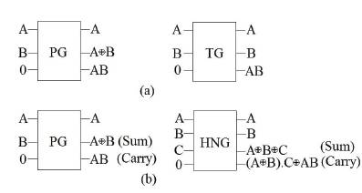
Figure 4. (a) AND Gate Realization using PG and TG Gates Respectively (b) Half and Full Adder Realization using PG and HNG Gate Respectively
There are two choices available for reversible AND gate implementation. Four AND gates are placed at Level 1, Level 2, Level 4 and Level 6. At each level, three TG and one PG gates are used. The selection of TG gate is based on the fact that both inputs and AND functionality i.e., XiYj (i=0, 1, 2 and j=0, 1, 2, 3) is needed at the output for further processing. A PG gate is selected to obtain X3 Yj (j = 0, 1, 2, 3), as only AND functionality is needed at its output and its cost is less than TG gate. A complete realization of the proposed reversible multiplier is shown in Figure 5. As the Braun multiplier is modular, the proposed design can be extended to generalized n-bit reversible Braun multiplier by cascading more levels of adders and AND gates to the design of Figure 5.
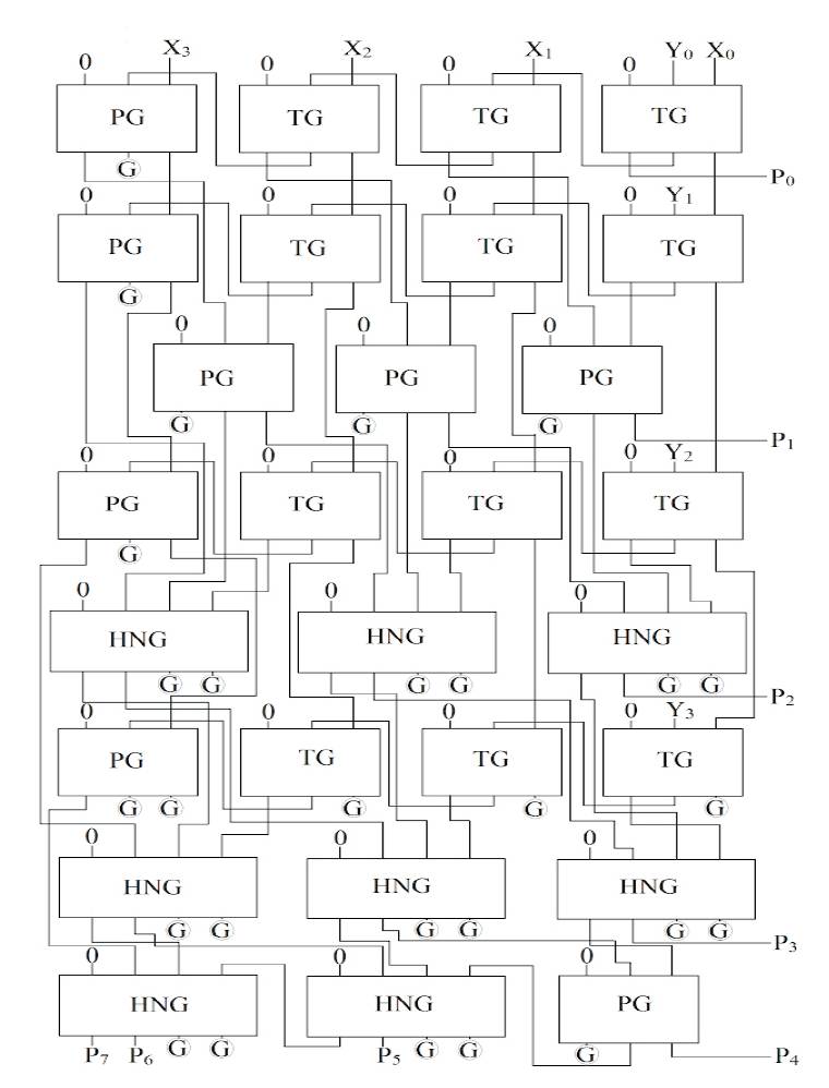
Figure 5. Proposed 4-Bit Reversible Braun Multiplier
The proposed 4x4 reversible Braun multiplier design uses PG, TG and HNG gates having quantum cost of 4, 5 and 6 respectively. The number of PG, TG and HNG gates is totaled to 8, 12 and 8 respectively. Thus overall reversible gates count is 28 (8+12+8). Considering the quantum cost of an individual reversible gate, the total quantum cost of the proposed design is computed as 140 (8x4+12x5+8x6). Since one input is kept constant in all the reversible gates, therefore the total number of constant inputs is 28 in the proposed design. The outputs encircled by G in Figure 5 are not used for further processing and are garbage outputs. Counting such outputs gives a total number of 28 garbage outputs. As, the total cost of the design is the sum total of all these four parameters, hence, the total cost of the proposed 4x4 reversible Braun multiplier is 224 (140+28+28+28). The performance parameters of the design are quantum cost, number of constant inputs, number of garbage outputs, and the total number of gates. A qualitative comparison is placed in the following section.
The proposed 4x4 reversible Braun multiplier is compared with an existing reversible multiplier design on the basis of quantum cost, number of constant inputs, number of garbage outputs and the total number of gates used in the design. The observations are summarized in Table 2. It can be inferred from Table 2 that, the proposed multiplier design proves more efficient as compared to other proposed multiplier designs in terms of total cost. The overall total cost of the proposed 4-bit reversible Braun multiplier design in 224 is better than the existing multiplier designs. The proposed design also has minimal number of garbage outputs and the constant inputs equaling 28. Hence, the proposed multiplier is cost efficient. Additionally, the proposed design can easily be extended to any generalized n-bit reversible Braun multiplier by cascading adders and single bit multipliers to the adder and multiplier rows of the proposed design. Two designs of reversible multiplier design are available in (Haghparast et al., 2008). It requires FG gates in order to propagate input bit X3 through the multiplier. Therefore, the total cost of the design proposed by Haghparast et al., 2008 in Table 2 differ from the one claimed in the paper. This problem (Haghparast et al., 2008) is also reported by Moallem & Ehsanpour 2013.
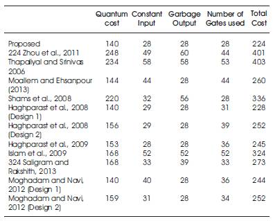
Table 2. Comparison Analysis of Proposed Reversible Multiplier
A 4x4 bit binary Braun multiplier has been analyzed and its reversible counterpart is proposed and designed in this paper. Braun multiplier is a simple parallel array multiplier which is used for unsigned numbers multiplication i.e., it is suited for positive operands. All the partial products are computed in parallel, and they are finally collected through a cascade of carry save adders. The architecture of Braun multiplier is iterative, so the proposed design can be extended to get a generalized binary Braun multiplier of any order n by adding additional reversible gates. PG, TG and HNG gates had been used in the proposed multiplier design. PG gates are used to realize AND gates in reversible computing domain, similarly HNG gates are used to realize full adders. TG gates are used to realize some of the AND gates and half adders in reversible computing domain. The multiplier design was found to be more efficient in terms of various optimizing parameters, which includes quantum cost, number of constant input lines, number of garbage outputs and total number of reversible gates than the previously proposed multiplier design, which are currently present in the literature. Instead of using multiple modules for partial product generation and addition, a single block of different reversible gates which do not require any logical shift register for shifting the partial products generated is used.