Figure 1. Single Ended SRAM Cell
SRAM (Static Random Access Memory) is a type of semiconductor memory that operates on a principle of Bistable Latching to store a bit of information. As the size of CMOS technology scales down to deep submicron region, power dissipation becomes a major issue in the VLSI design. The leakage power becomes dominant due to the second order effects of the transistors in deep submicron region. The leakage power aids in considerable increase of the total power dissipation of the device. The existing SRAM cells at submicron region dissipate more power and become unstable inspite of applying low power techniques like multi-threshold logic, body biasing techniques, stacked structures etc. This paper concentrates on the design of stable single ended SRAM array using power gating technique. The designs are developed and analyzed for different nm technologies using Digital Schematic and Microwind Tools. By using same tools, the Gated VDD technique based SRAM is analyzed to reduce the leakage power. The reduction in voltage swing results in reduction of dynamic power dissipation. The SRAM arrays for 2x2 and 4x4 arrays were developed using both 5T (or single ended) and Gated VDD 5T SRAM cells. The power dissipation at 90nm technology is reduced by 35% and 55.3% for gated 2x2 and 4x4 SRAM arrays respectively, when compared to single ended 2x2 and 4x4 SRAM arrays.
Power consumption is one of the main concerns of Very Large Scale Integration (VLSI) circuit design technology, for which Complementary Metal Oxide Semiconductor (CMOS) is the basic elementary component. Today's focus on low power is not only because of the recent growing demands of mobile and laptop applications. Even before the mobile era, power consumption has been a fundamental problem. Power consumption of CMOS consists of two components, dynamic and static [8]. Although dynamic power accounted for 90% or more of the total chip power previously, as the technology scale down to 65nm and 45 nm, static power has become a great problem for today's technology. Static power is a leakage power when the CMOS transistor is in sleep-mode [9], [10], [11].
One of the main reasons for the increase in leakage power is increase of sub-threshold leakage power. When technology feature size scales down [17], [18], supply voltage and threshold voltage also scale down. Sub threshold leakage power increases exponentially as the threshold voltage decreases. Furthermore, the structure of the short channel device decreases the threshold voltage even lower. Another contributor to static leakage power is gate-oxide leakage power due to the tunneling current through the gate-oxide insulator. Dynamic power dissipation depends on the operating frequency, power supply and the swing voltage during the active mode of operation. As the frequency increases the dynamic power dissipation also increases [12], [13], [14]. So high speed devices dissipate more dynamic power.
The memories are used to store the necessary data in any device like operating system, application programs, etc. Generally ROM is used to store the operating system software and some application programs. RAM is used to store the data that is frequently modified and stored. Even though many types of memories exist, SRAM is chosen for portable devices due to its stability and ease of operation [7] [8]. The stability of SRAM defines the amount of time it can store the written data.
Section 1 explains the objective of the paper and Section 2 discusses about the existing SRAM. The power gating technique based SRAM cell [3] [5] design to reduce the power at deep submicron region is discussed in Section 3.
The Section 4 deals with the design of arrays using the developed single bit SRAMs. The results are discussed in Section 5. Finally the paper is concluded.
The objective of this paper is to develop a low power design for memories that can be used in portable devices. The study includes investigation of scaling effects, SRAM cell designs, low power techniques that are suited for memories. Most low power techniques suited for memories include stacking, multi threshold, dual VT, etc. The methodology is based on development of first a single memory cell which is stable and has good noise margin. Further a low power technique best suited for the developed memory cell has to be chosen and verified. Finally the memory cell with low power technique can be used to develop arrays which are capable of storing multiple bits. Here initially a single ended SRAM cell is developed, then power gating technique is used which reduced the power dissipation significantly. Finally the 2x2, 4x4 and 8x8 arrays are developed and here each memory cell has the low power technique applied, so maximum reduction in power has been observed.
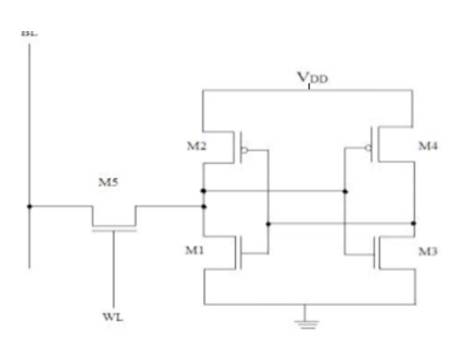
The existing SRAM cell designs [2] require Bit Line bar supply in addition to Bit Line and Word Line to read and write the data bit into the SRAM cell. This additional bit increases power dissipation and many portable applications do not require inverted output. Hence the inverted Bit Line and the corresponding transistor are removed to develop single ended SRAM. But still the outputs can be obtained for Q and Qbar as shown in Figure 1.
Figure 1. Single Ended SRAM Cell
This design provides the same stability as that of conventional 6T SRAM Cell for both read and write operation. The schematic of Single ended 5T SRAM Cell [1] is shown in Figure 2 and the corresponding layout at 120nm is shown in Figure 3.
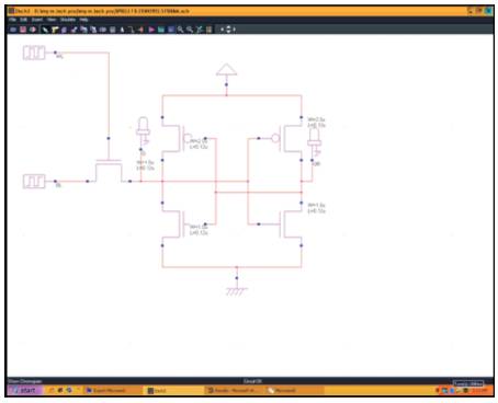
Figure 2. Schematic of 5T SRAM Cell
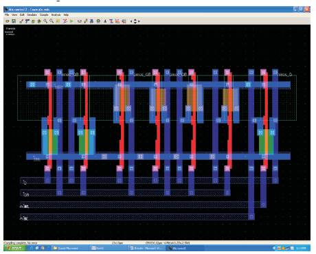
Figure 3. Layout of 5T SRAM Cell
The single ended SRAM cell uses only five transistors, hence occupies less area. As the additional inverted Bit Line is not used, the power dissipation is also decreased.
The 5T SRAM operates as a single ended SRAM Cell as the inverted bit line is not considered. Consider the pass transistor as M5 and the pull up transistors as M2 and M4 connected to outputs Q and Qbar respectively and the corresponding nmos transistors as M1 and M3. The 5T SRAM operates as when both bit line and word line are active Q is at Logic 1, then M3 turns ON and Qbar will be at Logic 0. If WL=0 and BL=1, the Q=0 and as M4 turns ON which makes Qbar=1.
In this technique, an extra transistor in the supply voltage or the ground of the 5T SRAM cell is added as shown in Figure 4. It turn on in the used section and turn off in unused section, so the cell's supply voltage is gated. The main reason behind the reduction in leakage current is stacking effect of self reverse-biasing series-connected transistors. This technique maintains both lower supply and threshold voltage while reducing leakage current. Gated-VDD transistor must be large enough to sink the current through SRAM cell, but a large transistor may reduce the stacking effect and also increase the area overhead. So, here a trade-off between area over head and leakage reduction [15], [16].
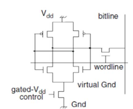
Figure 4. 5T SRAM Cell with an nMOS Gated - VDD
There exists a tradeoff between NMOS and PMOS Gated VDD transistor i.e., by Using NMOS transistor as Gated-VDD [4] [6], it reduce standby leakage current through stacking effect of three series connected NMOS transistor between Bit Lines and ground. Alternatively, using PMOS transistor it reduces required transistor width and thereby reduce area overhead, and also it does not provide the isolation between the bit Lines and the ground as NMOS, reducing energy saving.
NMOS gated-VDD impact on cell performance while PMOS do not significantly impact on the cell performance. There is a fundamental trade-off between reduction in leakage, transistor switching speed and area overhead of gated-VDD transistor.
The schematic diagram of Gated - VDD based 5T SRAM Cell is shown in Figure 5. And the developed layout at 120nm for Gated - VDD based 5T SRAM Cell is shown in Figure 6.
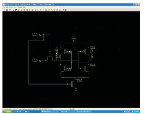
Figure 5. Schematic of Gated - VDD based 5T SRAM Cell
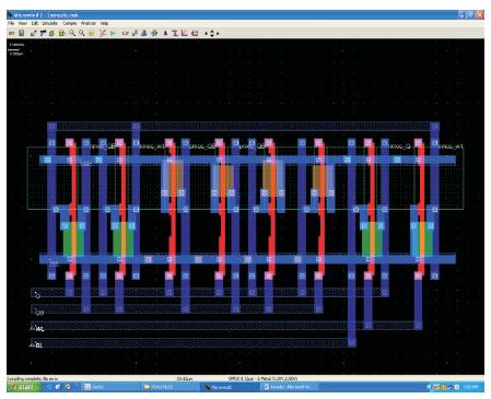
Figure 6. Layout of Gated - VDD based 5T SRAM Cell
The memories practically correspond to arrays where the designed transistors are arranged in the form of arrays and are accessed using row and column decoders. The 5T SRAM based designs without and with Gated – VDD technique can be developed.
The Schematic and layout at 120nm technology for 2x2 arrays are shown in Figures 7 and 8 respectively. The 2X2 array has a capacity of storing 4K Bits.
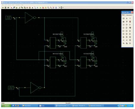
Figure 7. Schematic of 2x2 5T-SRAM Array
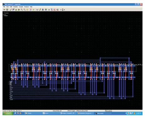
Figure 8. Layout of 2x2 5T-SRAM Array
The Schematic and layout at 120nm technology for 4x4 array are shown in Figures 9 and 10 respectively and 4X4 array has a capacity of storing 16K Bits.
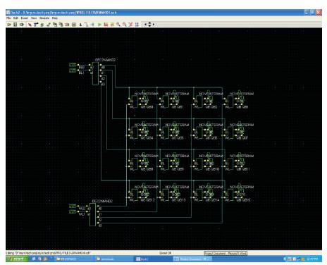
Figure 9. Schematic of 4x4 5T-SRAM Array
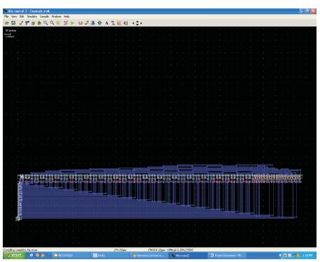
Figure 10. Layout of 4x4 5T-SRAM Array
The Schematic and layout at 120nm technology for 8x8 array are shown in Figures 11 and 12 respectively. The 8X8 array has a capacity of storing 64K Bits. The area increases slightly due to Gated VDD Technique.
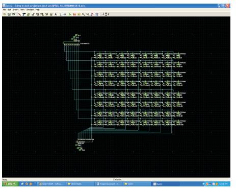
Figure 11. Schematic of 8x8 5T-SRAM Array
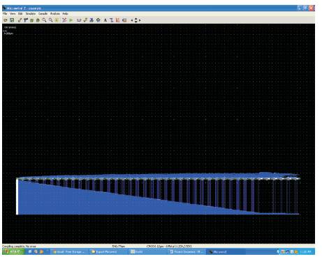
Figure 12. Layout of 8x8 5T-SRAM Array
The designs of single ended and Gated – VDD based SRAMs are developed, Verified and analyzed using DSCH (Digital Schematic) and Microwind Tool. The DSCH Tool was used to develop the schematics of SRAM designs. The Microwind Tool was used to draw the layouts at different technologies like 180nm, 120nm, 90nm, etc.
The simulation results for 2x2 and 4x4 SRAM arrays are shown in Figures 13 and 14 respectively. Here the corresponding bits are accessed only if the required bit and word lines are activated or held at logic '1'.
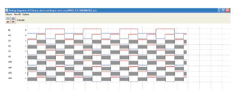
Figure 13. Simulation Result of 5T SRAM based 2X2 Array
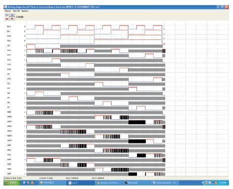
Figure 14. Simulation Result of 5T SRAM based 4X4 Array
Table 1 shows the comparison of power dissipation of 2X2 and 4X4 arrays at different nanometer technologies without and with Gated VDD Technique. From this table, it is clear that the Gated VDD Technique dissipates less power than normal arrays at different nanometer technologies.
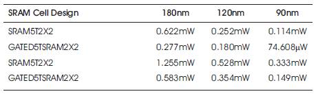
Table 1. Comparison of Power Dissipation of 2x2 and 4X4 Arrays at Various Technologies
The comparison of 2X2 array without and with low power technique is shown in Figure 15 and the percentage decrease in power dissipation by using Gated VDD technique is nearly 35% at 90nm technology.
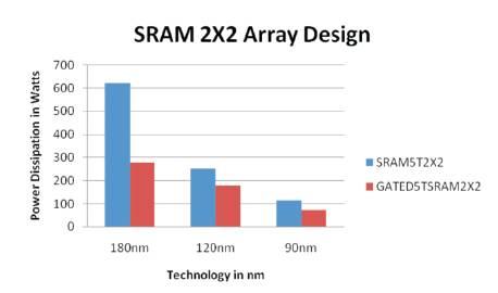
Figure 15. Comparison of 2X2 5T SRAM Without and With Gated VDD Technique Designs at 180nm,120nm and 90nm Technologies
The comparison of 4X4 array without and with low power technique is shown in Figure 16 and the percentage decrease in power dissipation by using Gated VDD technique is nearly 55.3% at 90nm technology. Hence as the array size increases, the power dissipation is decreased further.
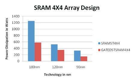
Figure 16. Comparison of 4X4 5T SRAM Without and With Gated VDD Technique Designs at 180nm,120nm and 90nm Technologies
As the size of CMOS technology scales down to deep submicron region, power dissipation becomes a major issue in the VLSI design. In this paper, a low area, low power and stable 5T SRAM cell is analyzed at submicron regions. The 5T SRAM cell acts as a single ended SRAM with good noise margin. The designs are analyzed for different nm technologies using Digital Schematic and Microwind Tools. By using same tools, the Gated VDD technique based SRAM was analyzed to reduce the leakage power. The reduction in voltage swing results in reduction of dynamic power dissipation. The Gated VDD 5T SRAM cell has a pull-down transistor connected to virtual GND, which reduces the subthreshold leakage current when the corresponding pull-up transistors of the cell is in OFF condition. Hence this reduces the static power dissipation also in the SRAM cell. The Voltage sources used in the design also increase the static noise margin of the Gated VDD 5T SRAM cell. Thus, in the Gated VDD SRAM cell both types of power consumption have been reduced for write operations. The SRAM arrays for 2x2 and 4x4 arrays were developed using both 5T and Gated VDD 5T SRAM cells. The power dissipation is decreased in Gated-VDD based 5T SRAM arrays by 35% in 2x2 array and 55.3% in 4x4 arrays when compared to single ended SRAM arrays at 90nm technology. Hence, the Gated VDD based 5T SRAM cell can be used in memories as a low power solution in battery operated devices like laptops, mobile phones, biometric devices etc.