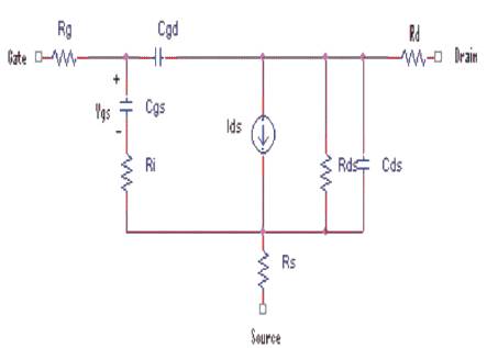
Figure 1. Equivalent Circuit of HEMT
The next generation of logic gate devices is expected to depend upon radically new technologies mainly due to the increasing difficulties and limitations of existing MOS technology. The high electron mobility transistor (HEMT) should ideally be the best device to work for high performance VLSI circuit design. This paper enumerates the design of high speed logic gates NOR, NAND, and NOT using AlGaN/GaN high electron mobility transistor (HEMT). This high electron mobility transistor is a novel device that is projected to outperform scaled CMOS technologies. The high electron mobility transistor based devices offers high mobility, high carrier velocity for fast switching. The p-type or n-type switching behavior depends upon the polarity gate voltage. The logic gates are designed by TTL logic, so the power consumption is less in this logic gates. It can be efficiently used in VLSI ICs. PSPICE simulations have been performed on the logic gates designed using both these technologies and their output behaviors have been extensively studied at different supply voltages keeping the designs at room temperature. The performances are evaluated in terms of power, delay and PDP to show that it is possible to reduce the delay and power consumption of the logic gates by replacing the CMOS transistors of the design with the emerging high electron mobility transistor(HEMT). The simulation results of the proposed logic gates appear to have better speed of operation. It can be suitable for SPICE simulation of hybrid digital ICs.
High-speed optical transmission systems are expected to play important roles in future broadband communication networks. In the systems, logic gates, which are required to operate in the gigabit data rate region are key components. This paper reports the circuit configuration and performance of logic gates. The model of AlGaN/GaN HEMT have been developed [1]-[6], [10], [11],and [12]. The model parameters of HEMT are shown in Table 1. Using these parameters, author created the PSPICE model of HEMT. The model can be implemented easily into the popular program SPICE for circuit simulations. Based on the model, NAND, NOR, NOT gates has been built and tested. In this paper, author designed logic gates using TTL logic, So the number of transistors used for making logic gates is very less and the area of gates is also reduced.
To design logic gate circuits using AlGaN/GaN High Electron Mobility Transistor (HEMT). To increase switching speed and power reduction of logic gates circuits designed using AlGaN/GaN high electron mobility transistor (HEMT). In this paper, PSPICE simulator is used for simulating logic gates. The model of HEMT is created by using above mentioned reference and some parameters are calculated manually. At the same time MOSFET based logic gate are simulated and then compared with HEMT.
Like other FETs, HEMT are used in integrated circuits as digital on-off switch. FETs can also be used as amplifiers for large amount of current using a small voltage as a control signals. Both of these are made possible by the FET's unique current-voltage characteristics. HEMT are heterojunctions. This means that the semiconductors have dissimilar band gaps. When a heterojunction is formed, the conduction band and the valence band throughout the material must bend in order to form a continuous level.
AlGaN/GaN HEMT exceptional carrier mobility and switching speed come from the following conditions. The wide band gap element is doped with donor atoms, thus it has excess electrons in its conduction band. These electrons will diffuse to adjacent narrow band gap material's conduction band due to the availability of states with lower energy. The movement of electrons will cause changes in potential and thus an electric field between the materials. The electric field will push the electrons back to the wide band gap element's conduction band. The diffusion process continues until the electron diffusion and electron drift balance each other, creating a junction at equilibrium is similar to a p-n junction. Note that, the undoped narrow band gap material now has excess majority charge carriers. Because the charge carriers are majority carriers yields high switching speed, and the fact that the lower band gap semiconductor is undoped means that there are no donor atoms to cause scattering and thus yields high mobility.
An important aspect of HEMT is that the band discontinuities across the conduction and valence bands can modifies separately. This allows the type of carriers in and out of the devices to be controlled. The HEMTs requires electrons to be the main carriers, a doping can be applied in one of the materials making the conduction band discontinuously smaller, and keeping the valence band discontinuously the same. This diffusion of carriers leads to accumulation of electrons along the boundary of the two regions inside the narrow band gap material. This accumulation of electrons leads to a very high current in these devices. The electrons are also known as 2 DEG or two dimension electron gas. In this paper, the model of HEMT have been developed from [1]-[6], [10], [11] and [12]. The equivalent circuit of HEMT is shown in Figure 1 and the parameters used for the design is shown in Table 1.
Figure 1. Equivalent Circuit of HEMT
Table 1. Parameters of HEMT
We designed the following logic gates using high speed HEMT (i) NOT, (ii)NAND (iii) NOR gates.
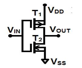
Figure 2. Circuit Diagram of NOT Gate Using HEMT
Figure 2 shows the implementation of inverter using HEMT. An inverter circuit outputs a voltage representing the opposite logic-level to its input level. A HEMT inverter comprising of a pHEMT (T1) and a nHEMT (T2). Here the 2 HEMTs are coupled in series between a high voltage (VDD) and a low reference voltage VSS. When the input is high, the nHEMT (T2) is turned on, pulling the output to ground, whereas the pHEMT (T1) is turned off. When the input is low, the gate-source voltage of the nHEMT is below its threshold, so it is turned off and pHEMT is turned on to pull the output high. This configuration normally reduces power consumption since one of the transistors is always off in both logic states. Processing speed can be improved due to the relatively low resistance compared to the CMOS devices.
Digital electronics circuits operates at fixed voltage levels corresponding to a logical 0 or 1 (see Binary). The truth table of proposed NOT gate is shown in Table 2.

Table 2. Truth Table of NOT Gate
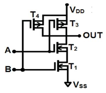
Figure 3. Circuit Diagram of Two Input NAND Gate Using HEMT
Figure 3 shows a NAND gate constructed using 4 HEMTs. Here the HEMTs act as switches. When both the inputs A and B are high, the nHEMTs (T1 and T2) are turned on to connect the output to ground. If any of the input is low, the path to ground is cut off and one of the pHEMTs (T3 and T4) turns on to connect the output to VDD. Adding more input terminals to a logic gate increases the number of input state possibilities which finds its application in designing flip flops, counters etc. The output will be high (approaching VDD) if all the two inputs or any one of the input is low (e.g., 0V), and the output will be low if all the two inputs are high (VDD). The truth table of proposed NAND gate is shown in Table 3.
Table 3. Truth Table of NAND Gate
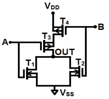
Figure 4. Circuit Diagram of Two Input NOR Gate Using HEMT
Figure 4 shows a NOR gate designed using HEMTs. It comprises of driver HEMTs (T3 and T4) coupled together in series between a high supply reference (VDD) and a parallel connected active load transistors (T1 and T2), which is coupled to a low supply reference VSS. The gates of the driver transistors T3 and T4 provide first (A) and second inputs (B) to the NOR gate and gate output (OUT) is taken out from the drain of parallel combination. If either input is low then the output is high, conversely, if both the inputs A and B are high then the output will be low. The truth table of proposed NOR gate is shown in Table 4.
Table 4. Truth Table of NOR Gate
To evaluate the performance of proposed logic gates NOT, NAND, NOR using HEMT technology. Simulations are carried out using PSPICE tool in nominal conditions with operating frequency at 2GHz. Transient analysis of the proposed logic gates using MODFET technology is shown in Figure 5, 6 and 7.
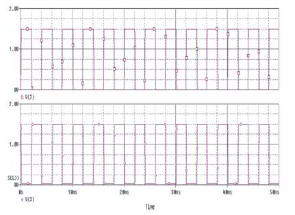
Figure 5. Simulation Results of NOT Gate Using HEMT
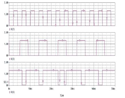
Figure 6. Simulation Results of NAND Gate Using HEMT
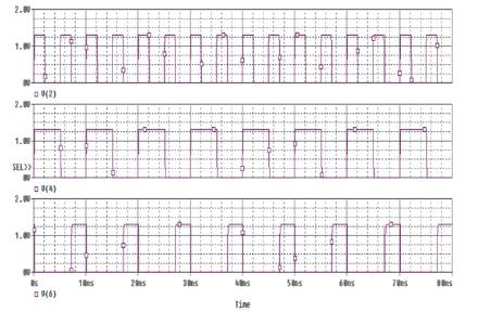
Figure 7. Simulation Results of NAND Gate Using HEMT
The proposed logic gates NOT, NAND and NOR using HEMT is designed and compared with existing logic gates. Each gate is optimized for power delay product. Simulation results for delay, power, PDP and area at nominal conditions for the logic gates are summarized in Table 5. and comparison graph is shown in Figure 8a, 8b, and 8c.
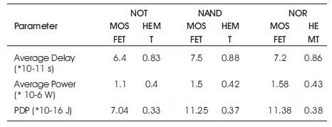
Table 5. Comparison of HEMT and MOSFET
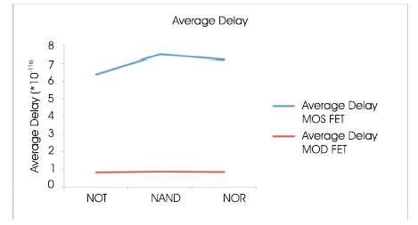
Figure 8a. Comparison of MOSFET and MODFET – Delay
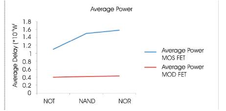
Figure 8b. Comparison of MOSFET and MODFET – Power
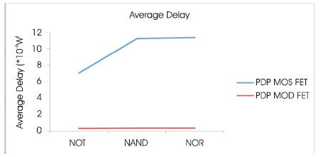
Figure 8c. Comparison of MOSFET and MODFET – PDP
In this paper, author have designed an efficient logic gates NOT, NAND and NOR using AlGan/Gan HEMT technologies. The logic gates are simulated in the PSPICE with operating voltage of 1.5V and operating frequency at 2GHz. HEMT logic gates have 65% less power consumption, delay also decreased and PDP(power delay product) has been reduced 80% than MOSFET design. The rise time and fall time has also been decreased. This work is also compared with other existing work [7], [8], [9]. The HEMT based logic gates is more efficient in average power, delay, PDP (power delay product). Hence the performance analysis of an efficient logic gates NOT, NAND and NOR using HEMT is more efficient for low power and high performance applications.
The author is grateful to the management of Sathyabama University, Chennai, especially to Dr.Jeppiaar, chancellor, Dr.Marie Johnson & Dr.Mariazeena Johnson, Directors for providing the necessary facilities for carrying out this research.