 The frequency of is twice, based on the frequency of Vpc and the input signal frequency is 1/2. The amplitude of Vpc and are 0–0.5V and 0–0.25V respectively. The frequencies of Vpc and are 10kHz and 20kHz.
Multiplication Algorithms have considerable effect on processors’ performance. Multiplier is an important circuit used in electronic industry especially in Digital Signal Processing operations such as filtering, convolution and analysis of frequency. There are different types of algorithms used in multipliers to achieve the better performance. In this paper, 8*8 Wallace Tree and Dadda multipliers are implemented using two phase clocking subthreshold adiabatic logic. Its power dissipation is less when compared to their respective 8*8 CMOS multipliers. This paper can be implemented in HSPICE using 0.18μm CMOS standard process technology.
To reduce the power consumption, the two existing low power technologies to be considered are Sub-threshold CMOS and Adiabatic logic. Sub-threshold CMOS theory is a technique which can reduce the power consumption to low threshold voltage than specified and Adiabatic logic circuit is a technique to reduce energy consumption by suppressing the voltage applied to the resistance of the circuit.
Multiplication is one of the arithmetic operations performed by the multiplier in various analog and digital circuits. It plays an essential role in computer Arithmetic operations for both general purpose and digital signal processors. The important parameters which should be taken into consideration in digital circuits are speed and power dissipation. In order to achieve energy efficient and low power VLSI (Very Large Scale Integration) circuits, different multiplication algorithms will be used to illustrate methods for designing different cells.
The proposed system (Two Phase Clocking Su threshold Adiabatic Logic) uses a two phase clocking power supply which has different frequency and amplitude. For example, a 2-chain inverter circuit is shown in Figure 1. The timing chart for the circuit is shown in Figure 2. It is necessary to switch on-off the input signal when Vpc and The frequency of is twice, based on the frequency of Vpc and the input signal frequency is 1/2. The amplitude of Vpc and are 0–0.5V and 0–0.25V respectively. The frequencies of Vpc and are 10kHz and 20kHz.
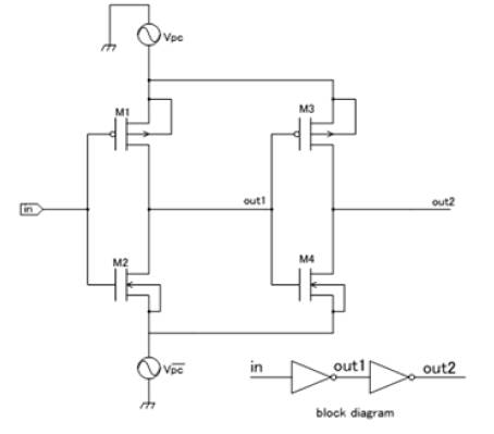
Figure 1. Cascaded Inverter
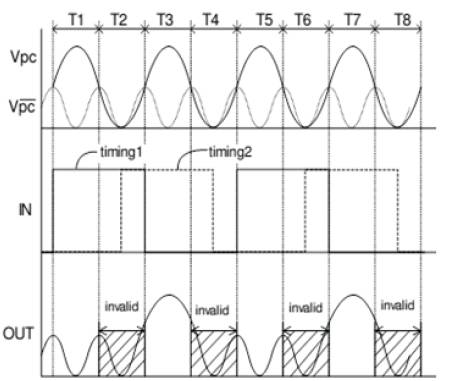
Figure 2. Timing Chart
C.S Wallace developed a fast process for multiplication of two numbers in the year 1964 (A suggestion for a fast multiplier). It is implemented by adders using parallel multiplication resulting in less delay. The Wallace method uses a three step process for the multiplication of two numbers.
Step 1: Multiply (logical AND) each bit of one of the arguments, by each bit of the other yielding in n2 results. Depending upon the position of the multiplied bits, the wires carry different weights. For example, the wire of a bit carrying result of a2 b3 is 32.
Step 2: Reduce the number of partial products to two layers of half adders and full adders.
Step 3: Group the wires in two numbers, and add them using a conventional adder. The partial product Dot diagram reduction for 8x8 Wallace Tree Multiplier is shown in Figure 3 (Design and Analysis of CMOS Based DADDA Multiplier).
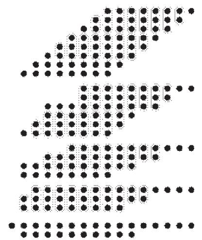
Figure 3. 8*8 Wallace Tree Multiplier
In the Wallace Tree method, three single bit signals are passed to a one bit full adder which is called a Three Input Wallace Tree circuit, and the output signal (sum) is supplied to the next stage full adder of the same bit, and the carry output signal thereof is passed to the next stage full adder of the same number of bit, and the carry output signal thereof is supplied to the next stage of the full adder located at a one bit higher position.
Luigi Dadda, the computer scientist has invented the DADDA hardware multiplier during 1965. DADDA multiplier is extracted form of parallel multiplier. It is slightly faster and requires fewer gates. Different types of schemes are used in parallel multiplier. The DADDA scheme is one of the parallel multiplier schemes that essentially minimizes the number of adder stages required to perform the summation of partial products. This is achieved by using half and full adders to reduce the number of rows in the matrix number of bits at each summation stage
Dadda multipliers are a refinement of the parallel multipliers presented by Wallace. The maximum height of each stage is determined by working back from final stage which consists of two rows of partial products. Each stage height should be in the order of 2,3,4,6,9,13,19,28,42,63 etc. Dadda multiplier consists of three stages same as in the Wallace Tree Multiplier.
The reduction process for a Dadda multiplier is developed using the following Recursive Algorithm (wikipedia).
The reduction process should be in such a way that after the final reduction step, number of rows should be two, as shown in last stage of Figure 4 (High performance dadda multiplier implementation using high speed carry select adder). The last row is obtained by just performing addition or passing the bits through adder blocks. The reduction process for above shown 8*8 Dot Algorithm can also be applied to 4*4 Dadda Multiplier. In this process, the minimum length should be 2. So, let c=2, and next size of the column is c =(3/2)*c ,by calculating this formula we get column sizes as 2,3,6,9,13........
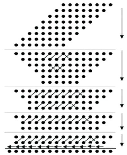
Figure 4. 8*8 Dadda Multiplier
In a 8*8 multiplier after rewriting the Dot Diagram, the maximum column size is 9, from the formula next column stage is 6, so after next reduction state, the maximum column size should be 6.
For that, the reduction process is as shown (A High speed floating point multiplier using vedic mathematics):
After these steps, all the columns will be less than or equal to 6. From the formula, next column size should be 4. So the following steps have to be taken.
Step 1: For first 4 columns, the size is less than or equal to 4.
Step 2: 5th column has 5 bits, in order to reduce it to 4, one half adder is required.
Step 3: 6th column has 6 bits and a extra carry bit from 5th column makes it a total of 7 bits, so two adders i.e. a full adder and a half adder are required.
Step 4: The columns from 7 to 11 have 6 bits and extra two carry bits coming from the previous stage, each column is reduced using two full adders.
Step 5: 12th column has four bits, but it will get two extra th carry bits from 11th column, so a full adder is required.
Now after this reduction, each and every column has less than or equal to 4 bits. From the formula, next column size has to be 3. The reduction steps are
Step 1: First three columns have 3 bits. So reduction is not necessary
Step 2: 4th column has 4 bits and to reduce it to 3 bits, a half adder is required.
Step 3: 5th to 12th columns have 4 bits and a extra carry bit coming from the previous stage which make the number of bits to 5, in order to reduce it to 3, a full adder is required.
Now after this reduction, each and every column has less than or equal to 3 bits. From the formula, next column size has to be two. The reduction steps are
Step1: First two columns have one and two bits respectively, so reduction is not required.
Step 2: 3rd column has four bits, and in order to reduce it, a half adder is required.
Step 3: 3rd to 13th columns have 3 bits and a extra carry bit coming from the previous stage which make the number of bits to 4, in order to reduce it to 3, a full adder is required.
Now after this reduction, each and every column has less than or equal to 2 bits. With this, the reduction process is completed. Then it is given to adder stage which will deliver the result. The number full adders in Dadda reduction be N2 - 4N+3. The number of halfadders will be N-1. Where N is the bit size of the multiplier.
For a 8*8 Dadda multiplier, the usage of resources is same as that of Wallace multiplier, but the operating time varies. As the critical path changes, delay is less than that of Wallace multiplier.
These multipliers were implemented and tested in HSPICE. The results are shown in Figure 5 obtained by simulating the code and the Power dissipation is tabulated in Table 1. Figure 6 shows the 8*8 CMOS Dadda Multiplier.
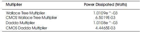
Table 1. Power Comparison of multipliers
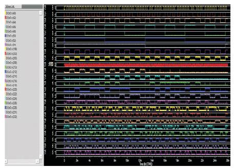
Figure 5. 8*8 Dadda Multiplier
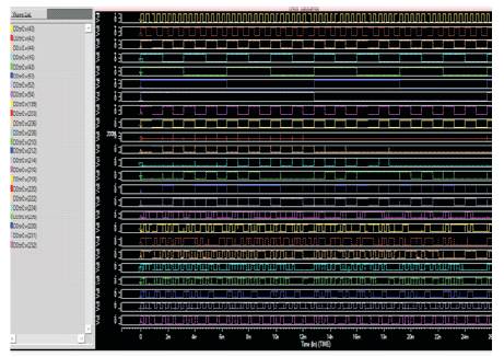
Figure 6. 8*8 CMOS Dadda Multiplier
This paper presents an effective implementation of Wallace Tree and Dadda multipliers using two phase clocking sub threshold Adiabatic Logic. The results of the multipliers implemented using this logic have been compared with respective CMOS multipliers and found that by using two phase clocking sub threshold adiabatic logic, power dissipated is less. The authors also found that Dadda multiplier has less power dissipation when compared to Wallace Tree Multiplier.