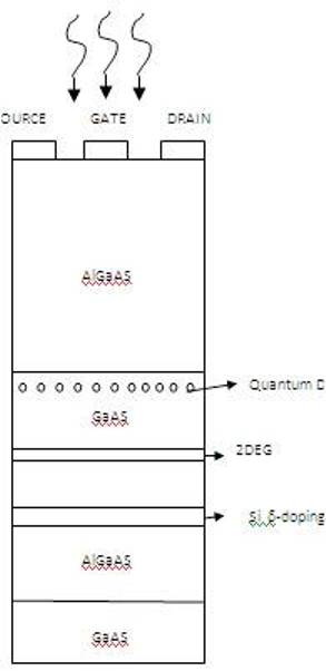
Figure 1. Schematic Diagram of Quantum Dot Transistor
The DC performance of the Quantum Dot Transistor under illumination is studied and presented in this paper. A device structure consisting of Quantum Dots(QD) in the GaAs layer is considered for illumination. The photoconductive effect in the GaAs and QD layer which increases the 2DEG Channel electron concentration is considered. The I-V Characteristics of Quantum Dot Transistor, under dark and illumination condition have been calculated, plotted and discussed. The Transfer Characteristics of Quantum Dot Transistor without and with illumination, Optical Response of Quantum Dot Transistor, and sheet concentration of the device is also calculated, plotted and discussed.
This paper demonstrates the study of optical effect in high speed device due to their potentiality in Fiber optical communication and optical integration. Some investigators have carried out both experimental and analytical studies G.E. Moore (2003), P. M. Zeitzoff et al (2005), L. Kouwenhoven et al (1998), L. I. Glazman (2000), J.M. Zamanillo, et al (2001), J.M. Zamanillo et al A (2001),. E. Kardynal et al (2004), A Rogalski (2003), MV. Ryzhii (2003) Lee, J. S et al (2011), Song et al (2011), Konstantatos et al.(2010), Bonaccorso, F. et al.(2010), Mueller et al (2010), V. I. Klimov(2010), KF Brennan et al (2000), Heinzel(2003). On the effect of illumination in GaAs MESFET, AlGaAs MODFET and QDT shows that there is significant effect of incident light on the electrical parameters of the device, but there is a lack of theoretical and experimental work describing the effect of illumination on Quantum Dot Transistors.
Optical detectors have been demonstrated recently, that they utilize the photoconductive gain associated with storing photo-generated charge carriers in the vicinity of a 2 Dimensional Electron Gas (2DEG) in specially designed Field Effect Transistors (FETs). Approaches to the charge storage in these detectors have included electronic confinement using metallic gates, naturally occurring defect centers in AlGaAs, and self-assembled quantum dots.
A Quantum Dot (QD) X. H. Su et al (2005) is a nanometer sized structure that is capable of trapping electrons in three dimensions. Quantum dots will become the backbone of future microelectronic and photonic devices. Because of their unique properties due to quantum confinement of electrons in 3-dimensions, this results in interesting electronic and optical properties.
Fabrication of QDs became possible by the development of epitaxial growth techniques for semiconductor hetero structures. Quantum dots (QDs) are often referred to as 'artificial Atoms' as they exhibit discrete energy levels in their electronic structure as Atoms do due to their small size. Quantum Dot Transistors V. Kannan et al (2004), N. Marjanovic et al (2006) may be the potential candidate for the future optoelectronic devices.
An elaborate analysis considering all effects resulting from optical illumination of Quantum Dot Transistors is a very complex task. However, by making some assumptions, a simplified analysis considering relevant photo effects can be modeled. In this paper, a simplified analysis to account for the photoconductive gain effect is described and from this, the change in the DC performance with illumination is estimated and presented. The current Voltage Characteristics of the device Quantum Dot Transistor, with illumination (Photo current) and without illuminations (dark current) are calculated, plotted and discussed. The Transfer Characteristics of Quantum Dot Transistor without and with illumination, Optical Response of Quantum Dot Transistor, and sheet concentration of the device is also calculated plotted and discussed.
The Quantum Dot Transistor structure considered for illumination is shown in Figure 1. It consists of a GaAs/AlGaAs modulation doped FET containing a layer of InAs quantum dots separated from the 2 Dimensional Electron Gas (2DEG) in the GaAs channel.
QD are fabricated in semiconductor material in such a way that a quasi-zero dimensional “dot" is formed. A QD behaves similarl to atoms and is often referred to as artificial atoms or giant atoms.
The source and drain electrodes are ohmic contacts and the gate electrode is a schottky-barrier junction. The major photo effects arising in the illumination of Quantum Dot Transistor are band to band absorption in the GaAs and AlGaAs layer generating hole electron pairs in these regions.
The doped AlGaAs barrier layers provide excess carriers to the GaAs quantum well and the quantum dot layer. The impurities in the doped AlGaAs layer provide electrons to the undoped GaAs layer, and the space charges.
Therefore, a quantum well is formed at the boundary of the undoped AlGaAs and the undoped GaAs layers. The thickness of the GaAs quantum well is about or less than the exciton Bohr radius(100Ao ).The electrons and holes in the GaAs quantum well are confined by the AlGaAs energy barrier, respectively.
One of the most important recent developments in semiconductors is the achievement of structures in which the electronic behavior is essentially 2 Dimensional (2D). This means that, at least for some phases of operation of the device, the carriers are confined in a potential such that their motion in one direction is restricted and thus is quantized, leaving only a two-dimensional momentum which characterizes motion in a plane normal to the confining potential (2DEG).
Thus capture of even a single photo-excited charge can produce a detectable change in the source-drain conductance. Absorption of a photon inside the semiconductor produces an electron-hole pair. One of these carriers can be captured by the quantum dot, thereby altering the height of the potential island in the adjacent 2DEG layer.
Upon illumination, the photo-excited hole will be attracted to the negatively charged quantum dot. Capture of a hole by the dot will reduce its negative potential and increase the local electron density in the 2DEG layer, thereby increasing the 2DEG conductance.
Figure 1. Schematic Diagram of Quantum Dot Transistor
An incident photon with appropriate energy creates an electron-hole pair in the GaAs absorbing layer. With a reverse bias applied to the gate, the electric field directs the electron to the 2DEG shown in Figure 1 and the hole to the Quantum Dots (QDs), where it is trapped. Two effects may be considered here. They are Photoconductive effect and Photovoltaic effect as follows.
When photons are absorbed only in the GaAs layer, an increase in the electrons concentration of the 2 DEG Channel occurs due to Photoconductive effect. When photons are absorbed in the AlGaAs layer also, then the photo current is due to Photovoltaic effect. In this work, the authors have considered only Photo conductive effect, ie the generation of electrons only in GaAs layer. The relevant dimensions and material considered in Quantum Dot Transistor are presented in Table 1.The photoconductive effect is dominant when the incident photon energy is equal to or greater than the GaAs band gap but smaller than the AlGaAs band gap(Eg1 < Eph < Eg2 ). Then the AlGaAs is transparent to the illumination and the dominant photo effect is the generation of photo electrons in the GaAs layer alone.
This photoconductive gain makes the device very sensitive to illumination with light of appropriate energy. The quantum efficiency is assumed as unity.
Photo electrons generated in the GaAs layer will be collected by 2DEG layer and will contribute to increase the source to drain current. The photo generated holes drifting towards Quantum Dots and to the semi insulating substrate will be capacitively coupled to the grounded source. An estimation of the increase in the electron concentration Δn in the 2DEG channel due to illumination in GaAs layer is estimated as S.M.Sze (1981), R.N.Simons (1987).
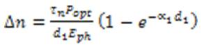
Where Popt is the incident optical power density, Eph is the incident photon energy, α1 the GaAs optical absorption coefficient and d1 is the thickness of the GaAs layer. τn is the electron life time.
The drain to source current due to photovoltaic effect is calculated as follows.
The photogenerated hole concentration Δp can be made using the expression [22].
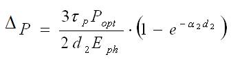
where Popt is the incident optical power density, Eph is the incident photon energy, α1 the GaAs optical absorption coefficient, d1 is the thickness of the GaAs layer and τp is the hole life time. Then the photovoltage Vph generated in the gate depletion region can be obtained by
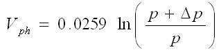
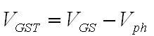
where  is the equilibrium hole concentration, ni is the intrinsic carrier concentration, n=ND is the donor impurity density of AlGaAs. The net voltage at the gate under illumination is a super position of the gate bias VGS and photovoltage Vph , given by
In this case, the AlGaAs is transparent to the illumination since the incident photon energy is lesser than the AlGaAs band gap and hence the dominant photo effect is the generation of photo electrons in the GaAs layer which alone is considered.

Table 1. Parameters Used for the Calculation
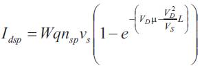
Assuming the saturation drift velocity of the photo electron as vs ,the drain to source photo current is Idsp in the linear region which is estimated as ,
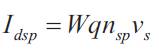
And the drain to source photocurrent in the saturation current can be estimated as
In this device, high Internal Quantum Efficiency (IQE) is achieved by using an electric field to direct the holes generated in the absorbing region of the detector to the QDs where ~70% are trapped.
The positively charged hole screens the bias field, effectively changing the gate bias by a positive amount and increases the channel current, Ids . This change in Ids caused by the addition of NQD positive charges to the QD plane is given by the expression.
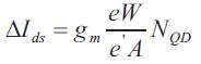
Where gm is the FET conductance, e is the charge , W is the ' distance between the gate and the QD layer , e is the permittivity of AlGaAs and A is the active area of the device. And the overall drain to source current due to illumination is
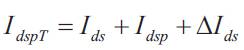
Where Ids is the drain to source current without illumination. Idsp is the drain to source photocurrent due to generation of electrons in the GaAs layer. ΔIds is the photocurrent due to Quantum Dots.
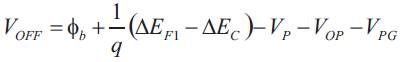
The offset voltage VOFF is calculated using the expression
where
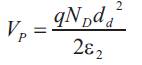
Vp is the pinch off voltage of the device,VOP is the photovoltage across the heterojunction and VPG is the voltage generated due to excess carriers.Also ΔEC is the conduction band edge discontinuity between AlGaAs and GaAs materials and EF is the Fermi energy.
The dimensions and other basic parameters used for calculation are given in Table 1. Numerical calculations have been carried out for Quantum Dot Transistor considering the optical effect.
The I-V characteristics of Quantum dot transistor under illumination and dark condition at Vg=0V and Vg=1V and Vg=2V are shown in Figure 2, Figure 3 and Figure 4 respectively.
The I-V characteristics of the Quantum Dot Transistor operated at various gate bias voltages illuminated with DC light is shown in Figure 5 at an optical power of Sopt =10mw.A tremendous increase in photo current is realized due to illumination in all the cases.
The I-V characteristics of the Quantum Dot Transistor operated at various gate bias voltages illuminated with DC light is shown in Figure 5 at an optical power of Sopt =10mw.A tremendous increase in photo current is realized due to illumination in all the cases. Also, an increase in the photo current is observed considering optical power. The optical response of the Quantum dot transistor under various optical power is shown in Figure 6. Figure 7 shows the Sheet concentration versus gate voltage plot which shows a tremendous increase in the sheet concentration that leads to an increase in photocurrent. The Transfer Characteristics of Quantum Dot Transistor without and with illumination is shown in Figure 8. An increase in photocurrent is absorbed due to illumination.
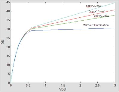
Figure 2. V-I Characteristics of Quantum Dot Transistor without and with illumination (Vg=0v)
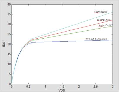
Figure 3. V-I Characteristics of Quantum Dot Transistor without and with illumination (Vg=-1v)
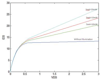
Figure 4. V-I Characteristics of Quantum Dot Transistor without and with illumination (Vg=-2v)
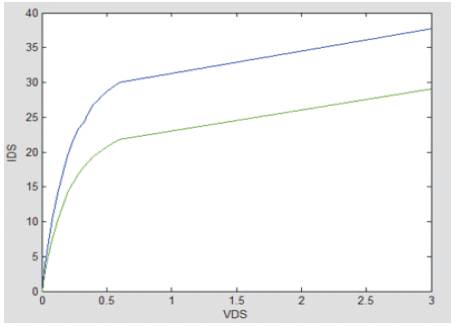
Figure 5. I-V Characteristics of Quantum Dot Transistor with illumination at VG=0V and VG=-1V at an optical power of Sopt =10mw
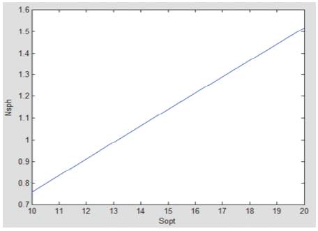
Figure 6. Optical Response of Quantum Dot Transistor (Sopt Vs Nsph )
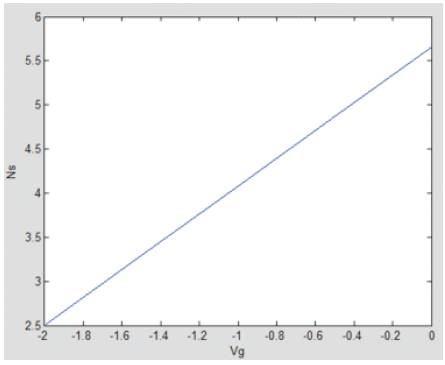
Figure 7. Sheet concentration versus gate voltage plot.
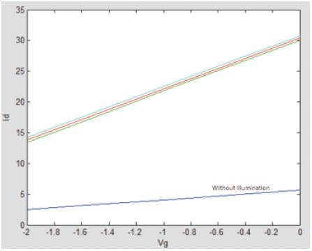
Figure 8. Transfer Characteristics of Quantum Dot Transistor without and with illumination (Vg Vs Id)
The characteristics of Nano structured Quantum Dot Transistor under front side illumination has been obtained and presented here. The offset voltage has been calculated with the effect of illumination. The I-V Characteristics of Quantum Dot Transistor under dark and illumination condition have been calculated, plotted and discussed. The Transfer Characteristics of Quantum Dot Transistor without and with illumination, Optical Response of Quantum Dot Transistor, and sheet concentration of the device is also calculated plotted and discussed. The I-V Characteristics have been compared with the experimental data, showing good agreement.