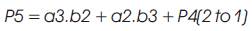
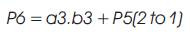
[1]
In this paper, the authors present an efficient implementation of Floating point multiplier which decreases delay of the circuit and this is done by replacing the multiplier block in the floating point multiplier and by comparing the delays in multiplication for each and every multiplier. In this paper, they use a standard floating point format i.e., IEEE 754 (which is a common standard for both Single Precision and Double Precision Floating point multipliers). Floating Point multiplication is an important factor in most DSP Applications. The other requirement of DSP applications in their fabrication is less area and low power consumption and less delay, also the performance matters in DSP systems. DSP systems require high performance. In this paper, the authors relate all the requirements of the DSP applications with respect to its speed. They have compared various multipliers as said before and have produced the best multiplier for floating point multiplication in terms of speed. This paper can be implemented using verilog HDL or VHDL and is checked in XILINX ISE 10.1 of FPGA.
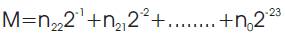
In DSP applications, the multiplication of floating point numbers have become an important requirement in a very large dynamic range i.e. FFT is a best example of DSP type, which involves multiplication of floating point number(in calculating real and imaginary terms).These floating point numbers are one of the best way of representing the real numbers in binary format. The floating point multiplication is done with reference to IEEE-754 format. This format supports both single precision floating point multipliers and double precision floating point multiplier. The IEEE 754 (IEEE 754-2008, IEEE Standard for Floating-Point Arithmetic, 2008) format supports two forms. They are: 1. Binary Interchange Format, 2.Decimal Interchange Format. It consists of three types of bits: (i) Sign bit, (ii) Exponent of 8 bits, (iii) multiplier result of 23 bits of fraction which is also called mantissa of 23 bit fraction. If another bit is added to the mantissa, it is called as significand. Exponent bits should be in the range between 0 and 255. If there exists a one in the MSB of the result of the significand, then it is called as Normalized number. The multiplier just gives the value of mantissa multiplication, it cannot implement anyone of the normalizing and rounding and overflow/underflow detections. So, the authors need to implement these blocks separately. The floating point multiplier is implemented in such a way that it implements overflow and underflow detections. Figure1 shows the format of single precision floating point numbers
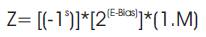
Where
Bias=127.
Two floating point multipliers can be multiplied in a sequence of 5 steps. They are
Step 1. Adding the powers of the numbers directly.
Step 2. Subtracting the value of bias from addition value.
Step 3. Multiplying the values of two mantissas
Step 4. Sign bit is calculated by performing the XOR operation on sign bits of both the numbers
Step 5. If the number is not normalized, the result has to be normalized
Figure 1. IEEE Single Precision Floating point Format
The Floating point form which is shown in equation (1) is the common form of Normalized Floating Point numbers. The algorithm for multiplying two floating point numbers is shown below
Step 1: Multiplying of mantissas; i.e., (M1*M2)
Step 2: Arranging the place of decimal point in the result
Step 3: Addition of Powers; i.e., (P1 +P2)
Step 4: Subtracting the Bias; i.e., (P1+P2 - Bias).
Step 5: Calculating the Sign; i.e., (S1 XOR S2 ).
Step 6: Result Normalization; i.e., obtaining one at MSB of signific and.
Step 7: Rounding the value (if necessary)
Step 8: Detection of Overflow and Underflow.
Block Diagram of Floating Point Multiplier is as shown in Figure 2.
Flowchart (Pardeep Sharma and Ajay pal Singh, July 2012) for Floating Point Multiplication is shown in Figure 3.
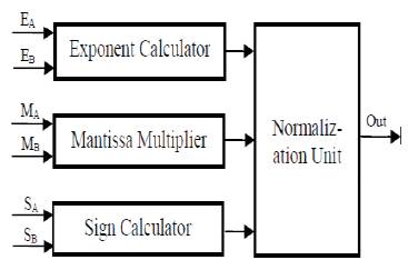
Figure 2. Block Diagram of Floating Point Multiplier
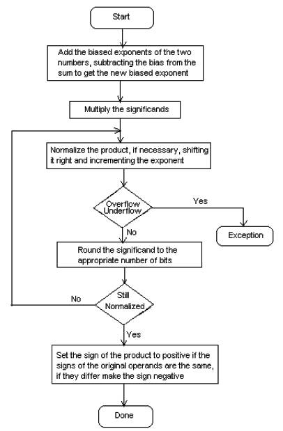
Figure 3. Flow chart for Floating Point Multiplication
An example for Floating Point Multiplication (Floating Point Arithematic by Jeremy R. Johnson, Anatole D. Ruslanov, William M. Mongan) is shown in Figure 3. First change the normal values to IEEE 754 single precision floating point format. Here they use a mantissa which is of four bits only
Binary representation of two numbers:
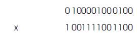
This binary representation is in IEEE 754 format. This IEEE 754 is a standard format for representing Single Precision binary floating point numbers. In this example, the authors consider the number of bits in mantissa to be 5. It should be anything between 1 and 23.
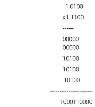
After the Placement of Decimal or radix point, the above number becomes 10.00110000
Biased Exponents
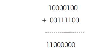
The above binary numbers show biased values for exponents.
True Exponents
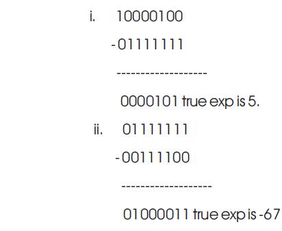
Adding true exponents: 5 + (-67) is -62
Subtracting Bias
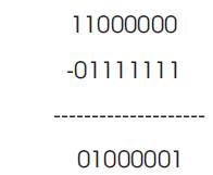
Re-bias exponent: -62 + 127 is 65. Unsigned representation for 65 is 01000001.
Combine the result back together (and add sign bit).
101000001 10.00110000.
Moving the radix point one place to the left increases the exponent by 1 if radix point moves to right exponent and decreases by 1 bit
1 01000001 10.00110000
after normalizing it becomes
1 01000010 1.000110000
The output value stored is as shown
1 01000010 00011
The above result will be obtained after rounding, as they specified the size of mantissa to be 5 bits.
The sign of result of the floating point multiplication can be found by performing the XOR operation on the signs of both the operands. If both the operands are same, then the sign of the output is also same. If both the operands are not equal, then the sign of output is negative.
The operation of exponent adder block is to add the exponents of the two floating point numbers and the Bias (127) is subtracted from the result to get true result.
i.e. EA + EB – bias.
The exponent is converted into 8 bit digital format and the addition is performed on two 8 bit exponents. In many of the designs, most of the computational time is spend in the significant multiplication process (multiplying 24 bits by 24bits); so quick result of the addition is not necessary. Thus the authors need a fast significant multiplier and a moderate exponent adder.
To perform addition of two 8-bit exponents, an 8-bit Ripple Carry Adder (RCA) is used. In Figure 4, the Ripple Carry Adder consists an array of one Half Adder, (HA) i.e., to which two LSB bits are fed and Full Adders (FA) i.e. to which two input bits and previous carry are given. Half Adder consists of two inputs and two outputs and Full Adder consists of three inputs (Ao, Bo, Ci) and two outputs (So, Co). The Carry Out (Co) from each adder is given to the next full adder i.e., each full adder has to wait until the carry out of the previous stage. The Block Diagram of RCA is shown in Figure 4.
After the exponent addition, bias is to be subtracted from the result. It is done as shown in Figure 5. Here, it is a Ripple Borrow Subtractor which performs the Bias Subtraction.
It involves an array of one subtractors and zero subtractors. The truth table for a one subtractor [4] is as shown in Tables 1 & 2.
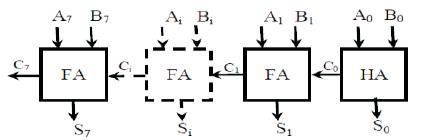
Figure 4. Ripple Carry Adder
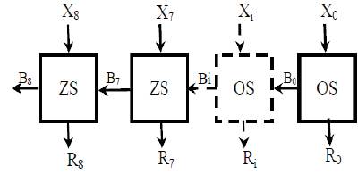
Figure 5. Bias Subtractor or Ripple Borrow Subtractor
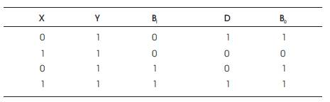
Table 1. One Subtractor Truth Table
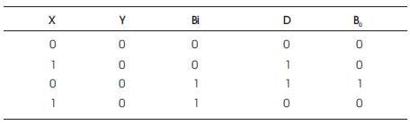
Table 2. Zero Subtractor Truth Table
Boolean equations are


The truth table for a Zero Subtractor is as shown below
Boolean equations are
Difference (D)=X XOR Bi.
Borrow(B)=NOT(X) AND Bi.
In this paper they mainly concentrate on the multiplier block which is to be designed in such a way that they need to careful in terms of hardware resources and speed of the device.
The multipliers compared are
1. Braun Multiplier
2. Wallace Tree Multiplier
3. Dadda Multiplier
4. Vedic Multiplier
Among the four Multipliers, Vedic multiplier exhibits less delay. The comparison process and description of multipliers is shown below:
As all other multipliers, Braun multiplier also involves 16 AND gates i.e., as 4*4 multiplier has 16 product terms. It consists of 12 full adders. Each Full adder has three inputs and two outputs, as the count of full adders increases delay in the circuit. So, in order to reduce this, they go for further designs. Figure 6 shows the 4*4 Braun Multiplier.
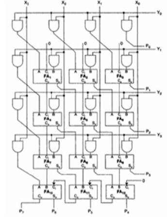
Figure 6. Braun Multiplier
The Wallace tree multiplier also involves 16 AND gates, as it has 16 product terms, i.e., for every 4 bit multiplier, it has 16 product terms. The partial product dot diagram for a wallace tree multiplier is shown in Figure 7.
Other than the AND gates, the Wallace tree multiplier has less number of full adders, when compared to Braun Multiplier. It has 8 full adders and 3 half adders, which significantly reduce delay.
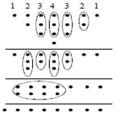
Figure 7. Wallace Tree Multiplier
Dadda proposed a sequence of matrix heights that are predetermined to give the minimum number of reduction stages. To reduce the N by N partial product matrix, Dadda Multiplier develops a sequence of matrix heights that are found by working back from the final two-row matrix. In order to realize the minimum number of reduction stages, the height of each intermediate matrix is limited to the least integer that is no more than 1.5 times the height of its successor. In fact, Dadda and Wallace multipliers have the same three steps
Step 1: Multiply (logical AND) each bit of one of the arguments, by each bit of the other, yielding n2 results. Depending upon the position of the multiplied bits, the wires carry different weights. For example, wire of bit carrying result of a b is 32.
Step 2: Reduce the number of partial products to two layers of full and half adders.
Step 3: Group the wires in two numbers, and add them with a convention adder. The partial product dot diagram reduction for Dadda Mulltiplier is shown in Figure 8.
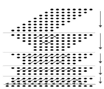
Figure 8. Dadda Multiplier
The process of reduction for a Dadda multiplier is developed using the following recursive algorithm (wikipedia)
The reduction process should be in such a way that after the final reduction step, number of rows should be two, as shown in last stage of Figure 10. The last row is obtained by just performing addition or passing through adder blocks. The reduction process for above shown 8*8 dot algorithm, can be applied to 4*4. In this process, the minimum length should be 2. So, let c i=2,and next size of the column is c i+1 =(3/2)*c i , by calculating this formula, we get column sizes as 2,3,6,9,13........
In a 8*8 multiplier after rewritting the dot diagram, the maximum column size is 9. From the formula next less column stage is 6, so after next reduction state the maximum column size should be 6.
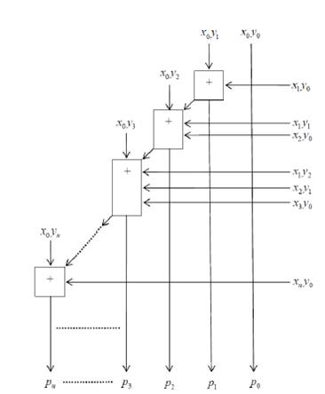
Figure 9. Vedic Multiplier
Figure 10. Normalizer
For that, reduction process is as shown:
After these steps, all the columns will be less than or equal to 6. From the formula, next column size should be 4. So the following steps have to be taken.
Step 1: For first 4 columns, the size is less than or equal to 4.
Step 2: 5th column has 5 bits In order to reduce it to 4, one half adder is required.
Step 3: 6th column has 6 bits and a extra carry bit from 5th column makes it a total of 7 bits, so two adders i.e;. A full adder and a half adder are required.
Step 4: The columns from 7 to 11 have 6 bits and extra two carry bits coming from the previous stage. Each column is reduced using two full adders.
Step 5: 12 thcolumn has four bits, but it will get two extra carry bits from 11th column, so a full adder is required.
Now after this reduction, each and every column has less than or equal to 4 bits. From the formula, next column size has to be three. The reduction steps are
Step 1: First three columns has 3 bits. So no reduction is necessary.
Step 2: 4th column has 4 bits and to reduce it to 3 bits,a half adder is required.
Step 3: 5th to 12th columns have 4 bits and a extra carry bit coming from the previous stage which make the number of bits to 5. In order to reduce it to 3, a full adder is required.
Now after this reduction, each and every column has less than or equal to 3 bits. From the formula, next column size has to be two.
The reduction steps are
Step1: First two columns have one and two bits respectively, so no reduction is required.
Step 2: 3rd column has four bits, and in order to reduce it, a half adder is required.
Step 3: 3rd to 13th columns has 3 bits and a extra carry bit coming from the previous stage which make the number of bits to 4. In order to reduce it to 3, a full adder is required
Now after this reduction, each and every column has less than or equal to 2 bits. With this, the reduction process is completed. Then it is given to adder stage which will deliver the result. The number of full adders in Dadda reduction be N2 -4N+3. The number of half adders will be N-1.
For a 4*4 Dadda multiplier, the usage of resources is same as that of wallace multiplier, but the operating time varies. As the critical path changes, delay is less than that of Wallace multiplier.
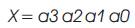
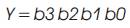
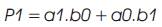
Vedic Mathematics is the ancient methodology of Indian mathematics which has a unique technique of calculations, based on 16 Sutras (Formulae). The idea for designing the multiplier is adopted from ancient Indian mathematics "Vedas” (Design of high speed Vedic multiplier using high speed mathematics techniques' International Journal of Scientific and Research Publications, March 2012). On account of those formulas, the partial products and sums are generated in one step which reduces the carry propagation from LSB to MSB The gifts of the ancient Indian mathematics in the world history of Mathematical Science are not well recognized. The contributions of Saint and Mathematician in the field of Number Theory, 'Sri Bharati Krishna Thirthaji Maharaja', in the form of Vedic Sutras (formulas) are significant for calculations. He had explored the mathematical potentials from Vedic primers and showed that the mathematical operations can be carried out mentally, to produce fast answers using the Sutras. In this paper, the authors are concentrating on “Urdhva tiryakbhyam” formulas and other formulas are beyond the scope of this paper. Urdhva tiryakbhyam Sutra is a general multiplication formula applicable to all cases of multiplication. It literally means “Vertically and Crosswise”. The proposed method of Urdhva Triyagbhyam can be implemented for binary system in the same way as decimal system. The 4 x 4 multiplication has been done in a single line in Urdhva method, whereas in shift and add method (Conventional), four partial products have to be added to get the result. This implies the increase in speed. Figure 3 shows the number of adders involved in Vedic multiplication. Vedic technique takes an edge over the conventional technique in the reduction of the number of adders used. The Vedic multiplication is implemented using the following equations. The equations for implementation are: The first four bit number is X, and second four bit number is y.


Vedic multiplier has less delay, when compared to other multipliers as it uses a different scheme for computations, i.e., for full and half adders. The Block diagram for a Vedic Multiplier is shown in Figure 9.
The result of the Mantissa multiplication is said to be normalized, if it has a leading 1 just to the left of the decimal point. Since the inputs are normalized numbers, then the intermediate product has the leading one at bit 46 or 47.
Step 1: If the leading one is at 46th bit, then the obtained product is already a normalized number and no shift is needed.
Step 2: If the leading one is at 47th bit, then the obtained product is shifted to the right and the exponent is incremented by 1.
The schematic diagram of a normalizer is shown in Figure 10.
Overflow/underflow indicates that the result's power value is too big/small to be represented in the power field. The power of the result must be 8 bits in size, and must be between 1 and 254, otherwise the value is not a normalized one. An overflow may occur while adding the two exponents or during normalization. Overflow in addition of exponents can be compensated during subtraction of the bias; resulting in a normal output value (normal operation). An underflow may occur while subtracting the bias to form the intermediate exponent. If the intermediate exponent < 0, then it's an underflow that can never be compensated; if the intermediate exponent = 0, then it's an underflow that may be compensated during normalization by adding 1 to it. Normally overflow/ underflow doesn't occur. They occur in worst case scenarios.
The overflow/underflow rules for detection and correction are shown in Table 3.
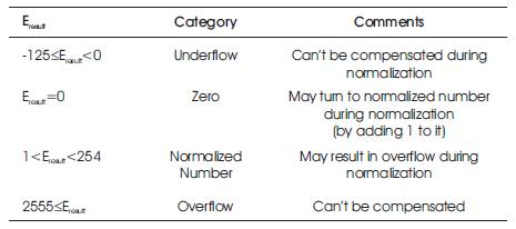
Table 3. Overflow and Underflow Detection
The pipelined (A High Speed Binary Floating Point Multiplier Using Dadda Algorithm) diagram is as shown in Figure 11.
This multiplier was implemented and tested in Xilinx ISE 10.1. It can be tested on Spartran 3E Virtex 5 of FPGA.
Earlier, this multiplier was tested in Xilinx ISE 10.1. To code the multiplier, the authors can use either of VHDL or Verilog HDL. By coding, they implement the multiplier. The tabular results shown in Table 4 are obtained by simulating the code in ISE 10.1. Parameters like Delay related to speed, number of LUTs used and number of slices related to area are tabulated. Results for various multipliers are shown in Table 4.
The delay of the normal Vedic multiplier is very less, when compared to the other multipliers. Here they compare all the four multipliers described and by simulating, they get the reults, which tells that floating point multiplier with vedic multiplier has less delay.
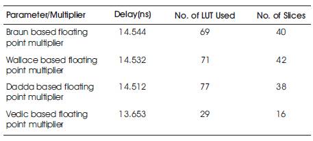
Table 4. Results of various floating point multipliers
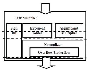
Figure 11. Pipelining stages
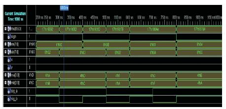
Figure 12. Results for Vedic Multipliers
The simulation of this floating point multiplier is performed on Xilinx ISE 10.1. This can be implemented on Spartran 3E of FPGA to obtain the same results. The simulation results for a Vedic multiplier are shown in Figure 12.
This paper presents an effective implementation of floating point multiplier which supports IEEE 754 single precision floating point format. Various multipliers have been implemented and on comparing the results, they found that floating point multiplication by using Vedic multiplier can be implemented with less delay. This has been implemented on Xilinx ISE 10.1.