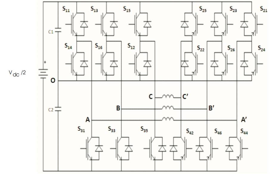
Figure1. Proposed New Topology of the Three level NPC inverter
An improved three level inverter scheme, with less number of switches, having the features of common mode voltage elimination, DC link capacitor voltage balancing, and minimization and equalization of voltage stress across the switches, for an open end winding induction motor drive, have been proposed in this paper. Open-end winding induction motor, when fed from its two ends by a three level inverter, suffers from the drawbacks of common mode voltage, which causes current to flow through its bearings along with the shaft and that type of capacitor voltage unbalance, causes current to flow through the neutral point. Further, such inverters require a large number of switches, which lead to higher switching losses and unequal voltage stress in the switches. A new inverter topology with less number of switches, that gets rid of the problems of common mode voltage and DC link capacitor voltage unbalance along with reduced and equalized voltage stresses in the switches, has been proposed in this paper. The simulation and the hardware results of the proposed topology show smoother output voltages across the machine phases.
Recently, there has been a growing popularity for multilevel inverters among the industries, for adjustable speed drives applications, because they offer speed control over a wide range. The Neutral Point Clamped (NPC) Multilevel Inverter is useful for high power drives with larger systems with considerable efficiency and capable of providing speed control over a wide range[1][14]. However, Neutral Point Clamped (NPC) Inverter suffers due to the drawback of capacitor voltage unbalance, which is caused by the variation of neutral point potential and its effect on load current, dc link capacitors etc., which has been analyzed using conventional methods[2]. A model, based on Direct – Quadrature (DQ) coordinate frame along with current switching functions for the drawbacks of common mode voltage and DC link capacitor voltage unbalance of NPC Multilevel Inverter scheme has been used to obtain the ripples in certain loading conditions[3]. To stabilize the neutral point voltage, a closed loop control system based scheme, which stores the voltage vectors in E-PROM, was formulated for line to line three phase voltage vector control and the neutral point potential was found to be varying within fixed limits[4], and a further simplified scheme was suggested, eliminating the capacitor voltage unbalance, using the switching pattern itself, and was found effective. It was an open loop method, which eliminated capacitor voltage unbalance in an effective manner[5].
A new NPC dual inverter topology, using conventional twotwo level inverters connected back to back, for an open end winding induction motor drive, which divided the entire space vector region into three parts, according to the speed range of the motor drive, was found effective[6]. Now a days Space Vector technique are popular and hence the relationship between the two was mathematically analysed and results were found out[7]. A three level inverter was implemented with the help of dual two level inverters fed from two different sources, with the common mode voltage being eliminated using a new switching strategy and thereby reducing bearing currents[8]. However, the requirement of two separate DC sources of equal value was a major drawback of the system, even though it has produced perfect smooth sinusoidal output.
Two new topologies, in which three level inverter was realized, by cascading two-two level inverters in different ways and both using only one source, with one topology using four rectifiers fed from only one source and the other using two rectifiers and two capacitors, with a scheme of using the redundant switching states, which were selected during vector rotation, were the gateway for new era of NPC Multilevel Inverters[9]. Though, the common mode voltages and currents were suppressed in this method, this work did not analyze the problem of DC link capacitor voltage balancing. Neutral point voltage variations in Second Topology[9] can be avoided by using the switching pattern itself and this idea was implemented by using the TMS320F24 processor, which eliminated the common mode voltage and the DC link capacitor voltage unbalance, by dividing switching vectors into six groups, out of them which only two groups were found to be useful to avoid Common Mode Voltage and the DC link capacitor voltage unbalance[10][13]. This method has the advantage of requirement of the capacitor voltage rating, which is nearly equal to the half of the conventional two level inverter and the capacitor of the DC link voltage balancing was made better by using a closed loop hysteresis controller, whose output was used to switch the inverter switches. But this topology had a disadvantage of having 24 switches. A new topology, where 24 switches were reduced to 18 switches, synthesized the same output voltage free from triplen harmonics, but with the drawbacks of having the certain restrictions on switching states, and not addressing the problem of DC link capacitor voltage unbalance was a noteworthy feature[11]. A new topology using this capacitor H-Bridge, comprising of 24 switches and 3 capacitors, which are bound to increase, if the number of levels increase, was a noteworthy work[12].
Dual multilevel inverter feeds the load, from both its sides, with (2n -1) levels of voltage across the phases, where n is the number of levels of voltages at the poles. Among the Neutral Point Clamped (NPC) inverters, dual inverters are popular, in which it is a conventional practice to synthesize the three level inverter by cascading the two numbers of two level inverters, with each arm of every two level inverter comprising of two switches. So, when two numbers of two level inverters are cascaded, 4 switches per arm are required [10]. In such topologies, the DC voltage source is assumed to be of Vdc/2 volts and hence for a three level inverter, two switches, one connected at the top side and other connected at the pole of the inverter, both are to be turned on for obtaining the positive voltage level Vdc/4 at the poles and two switches, one connected to neutral point and the other connected to a pole of the inverter, are to be turned on for obtaining zero level voltage(“0”) at the poles. But, for obtaining a negative voltage of - Vdc /4, only one switch below the pole is to be turned on. Under such conditions, the single switch, used for getting -Vdc /4, is subjected to larger stress, because the voltage across the MOSFET at the bottom is twice that of the other three IGBTs, causing the unequal voltage distribution across the IGBTs. In addition, the voltage requirements of the IGBT are increased.
However, on the visual inspection of the topology given in[10], it will be evident that cascading two numbers of two level inverters is not mandatory for synthesizing three level output voltage and only six switches per phase (three at one inverter and three at another), instead of eight switches are sufficient to produce the same results. The topology using only six switches per phase, using IGBTs, is shown in Figure 1, in which, all the switches, which were present just above the poles in the topology proposed in[10], have been removed, with the present one having only 18 switches. In this topology also the DC voltage source is assumed to be of Vdc/2 volts and hence, for synthesizing Vdc/4, 0,and - Vdc /4, the top switch, middle switch and the dc dc bottom switch should alone to be turned on, respectively. For example at pole A, to realize Vdc/4, only the switch S11 , for obtaining 0 volts only the switch S14 and for - Vdc/4 volts, only S21 alone to be turned on, respectively, and in general, the only one condition in this topology is that out of 3 switches connected to a particular pole, only one switch is to be turned on and the remaining two switches are to be turned off, by which, the voltage stress across the bottom switch is reduced and voltage distribution is made equal. Further, the same output of the topology proposed in[10], is obtained in a fair manner, with only 18 switches, the common mode voltage being eliminated easily and the DC link capacitor voltages being balanced.
Figure1. Proposed New Topology of the Three level NPC inverter
In an NPC topology, the first major issue is the common mode voltage, that refers to the sum of voltages at the poles of each side (i.e., the sum of voltages at A, B, C and the sum of voltages at A', B', C') of the inverter, being unequal, by which the windings of motor experience zero sequence currents flowing through them. So the sum of the voltages at the poles on each side should be made equal, to eliminate CMV. In a three level NPC inverter, the voltages at the poles may be Vdc /4, when it is connected across top capacitor C1, zero (0), when connected across neutral point and -Vdc/4, when connected across the bottom capacitor C2, through the corresponding IGBT switches, by which voltage across the phases are about 5 levels, which are -Vdc/4, -Vdc/2, 0, Vdc/4 and Vdc/2. The voltages to which the capacitors are charged, when connected to the corresponding points of the source are shown in Figure 2 with 'O' being the neutral point.
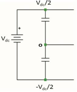
Figure 2. Voltage levels of capacitors
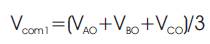
In the inverter topology, as shown in Figure1, the sum of voltages at the poles A,B,C are called as Common Mode Voltage (1) Vcom1 and is given by,
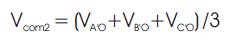
Similarly, the sum of voltages at poles A', B' and C' is called as Common Mode Voltage (2) Vcom2 and is given by,
Where,
VAO ,VBO , VCO , VA'O , VB'O, VC'O are the voltages of poles A,B,C,A',B' and C' with respect to neutral point 'O', respectively.
Hence, the Common Mode Voltage across the entire phase windings is given by,

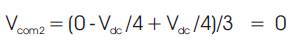
The switching combinations can be divided into following types of vectors.
(000, 0-+), the voltage at the poles at A,B and C are '0','0', '0', respectively. So, Common Mode Voltage Vcom1 from(1) is,
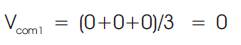
Similarly, voltages at A',B' and C' are '0', -Vdc /4 and Vdc /4 respectively. So, the Common Mode voltage Vcom2 from (2) is,
So Common Mode Voltage across the entire phases from (3) is ,
By, similar analysis, it can be found that that all the switching combinations are producing zero CMV at the inverter poles and across the phases and it is the only issue of capacitor voltage unbalance, which is going to decide the switching combinations to be chosen for switching the inverter switches, (Figure 3).
Figure 3. Switching Combinations of the proposed inverter topology
In an ideal neutral point clamped topology, it is expected that there should be no fluctuation of neutral point potential, for which the condition is that the DC link capacitor voltages should be equal; otherwise, current will flow through neutral point and will cause improper output voltages across the phases of the induction motor drive, which, in turn, may damage its insulation and windings. So, from the given voltage vector combinations, proper switching states are to be chosen, so as to achieve capacitor voltage balance and thereby making the neutral point potential zero.
In the small voltage vector OB' (000, 0-+), 0,0 and 0 volts are generated at the poles A, B and C and 0, - Vdc/4 and Vdc/4 volts are generated at the poles A', B' and C' respectively. From Figure 2, the induction motor phase winding connections are obtained as shown in Figure 4.
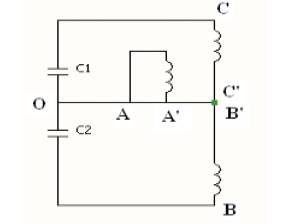
Figure 4. Winding Connections for Small Voltage Vector
This winding connection causes Capacitor C1 to charge and C2 to discharge, by which the small voltage vector seems to be a solution to the problem of capacitor voltage unbalance. However, it is evident that the small voltage vectors cause any one of the three phases to be short circuited across the neutral point and it is the A phase, which is short circuited, in the present case, and this may damage the corresponding winding phase and hence the small voltage vectors cannot be useful for switching the inverter for solving the problem of capacitor voltage unbalance.
By, similar analysis, the winding connections for all the other switching vectors have been obtained and shown in Figures 5 to 8.
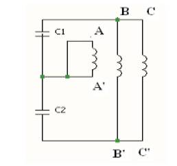
Figure 5. Winding Connections for Large Voltage Vector
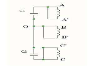
Figure 6. Winding Connections for Largel Voltage Vector
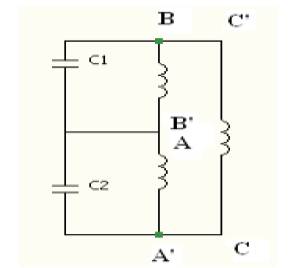
Figure 7. Winding Connections for Medium Voltage Vector
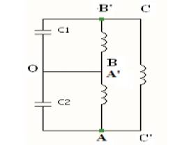
Figure 8.Winding Connections for Medium Voltage Vector
From Figure 7 and Figure 8, it is found that phases B and A are connected across the capacitors C1 and C2, respectively, and C phase winding is connected across both C1 and C2, with all of their corresponding terminals being reversed. So, C1, which was charged with the first switching combination, now discharges with the second switching combination and C2, which was discharging with the first switching combination, now charges with the second switching combination and hence, a medium voltage vector produces an effect in the second switching combination, which nullifies that of first one and hence charged capacitor discharges and discharged capacitor charges, due to the reversal of the winding connections, leading towards an easy solution to the problem of the capacitor voltage unbalance, which makes, the medium voltage vectors are suitable for both common mode voltage elimination and DC link capacitor voltage balancing.
This topology was simulated using MATLAB for an 0.5 HP induction motor. The DC source voltage was realized by a simple DC source of 100V and the capacitor values chosen were C1 = C2 =1000μF. The inverter was realized with the help of IGBTs. The simulation results are shown below.
It is found from Figure 9, that without using two inverters cascaded, and hence with the reduced number of switches, the same output voltage can be synthesized. The current through the motor phase winding is shown in Figure 10, which is a pure sinusoid. The DC link capacitor voltages Vc1 and Vc2 are shown in Figures 11 and 12 respectively. It is found that both the capacitor voltages are balanced. Figure 13 shows the gate signals for the switches connected to poles A and A'.
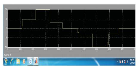
Figure 9. Output phase voltage
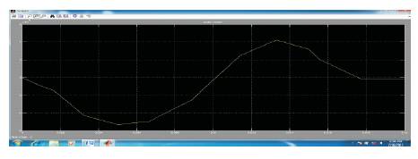
Figure 10. Current through motor phase
Figure 11. Voltage across C1
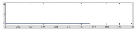
Figure 12. Voltage across C2
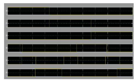
Figure 13. Gate Signals for switches connected at poles A and A'
The experimental verification of proposed topology was carried out using the prototype shown in Figure14. This topology was tested with V/f control with the DC link voltage being 115V and the voltage across each DC link capacitor being 57.5V. The DC link voltage balancing was implemented by using dsPIC30F4011 processor
The switches for the topology were of MOSFETs IRF 840, each of 8A rating. The multilevel output is shown in Figure 15, from which, it can be understood that a very good 5 level voltage across the output phases of the dual inverter can be obtained with lesser number of switches, without any restrictions as posed by the topology presented in [11].
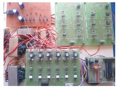
Figure 14. Experimental Setup of the proposed Topology
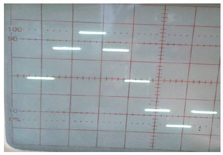
Figure 15. Phase Voltage
Thus, a new three level inverter topology with only 18 switches, for an open end winding induction motor has been proposed in this paper. Using a simple and effective method, the voltage across the switches are reduced and made equal, as only one switch in one arm is switched at a time, for synthesizing any of the three levels, with the output voltage being same as that of normal three level NPC inverter, and the problems of common mode voltage across the motor winding phases and DC link capacitor voltage unbalance being absent. The simulation using MATLAB and experimental verification of the above topology using hardware prototype was performed and the results also prove the same. The future scope of this research work is to obtain increased levels of output voltage with lesser number of switches.