(1)
A robust method for stabilizing Fully Differential (FD) two stage amplifiers is presented in Figure 2(c) which is fast, guaranteed latch free, low offset while offering simpler tracking of compensation with some increase in power dissipation. Submicron processes with supply voltages ranging from 0.7 to 1.2 V place an ever increasing demand for efficient use of analog supply budget headroom, Common Mode (CM) offset (VOSCM ), differential offset (Vos), and noise OSCM erode dynamic range. Common Mode (CM) offset is an often overlooked error contribution of the CM feedback amplifier. The desirable qualities of a CM amplifier are, fast settling, latch up free operation under all transient conditions while being low power, contributing low noise, low VOSCM to FD circuits, i.e. pipeline ADCs (Analog-to-Digital Convertors). It OSCM is widely known that, current feedback can be fast, limited only by the current gain bandwidth of the process [1,2]. The proposed CM current amplifier in Figure 2(c) avoids latching states while maintaining Common Mode FeedBack (CMFB) loop stability and simplifying CMFB compensation.
Fully differential two stage amplifiers are widely used as a result of increased dynamic range, attenuation of CM noise, reduced harmonic distortion, and increased bandwidth [2,3]. The major disadvantage of two stage fully differential circuits is their potential for latch up, the need for a fast CMFB circuit to set the CM output voltage, the added noise and the VOSCM contribution to system design considerations. The CMFB amp senses the output CM voltage from the FD amplifier and using negative feedback sets the CM voltage of the differential amplifier output to a CM reference voltage, VREFCM . In this paper, the authors investigate wide B and CM amplifiers for the highly desirable two stage amplifier in Figure 1 which has potential positive feedback and latch up [4,5]. Existing solutions reported as latch up free, [4,6] can add a degree of difficulty in compensation and/or in achieving necessary desired CM amplifier bandwidth while maintaining low VOSCM . Problems arise from the observation that, both CM st nd gain and FD gain share the identical 1st and 2nd stages and compensation, but with different transconductances (FD differential and CM pair) with an added CM gain stage. This difficulty is exacerbated when FD amplifier bandwidth approaches a process’s unity current gain bandwidth (fTA ). The proposed CMFB Current Amplifier (CMCA) addresses these difficulties using current feedback (M1CM) across the bandwidth of interest with the FD amplifier in context.
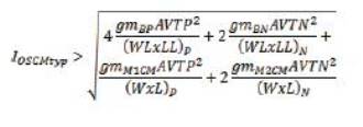
Figure 2 shows the CM amplifiers for FD amplifiers Figure 2.(a) and (b) are typical solutions[1]. It is clear from Figure 2 (a) and (b)that, only a fraction (IDN / (IDN + ISTAB )) of the total current is controlled by the CM loop. Classically, the role of the I current is threefold to provide the balance of the FD bias current, trimming offset currents and manage latch up [6,7]. CM offset current, IOSCM is a result of current mismatch between PMOS(P--type Metal Oxide Semiconductor) rail side currents (IP + IDP ) and NMOS(n-channel Metal-Oxide- Semiconductor Field-Effect Transistor) rail side (IN + ISTAB ) currents and CM amplifier VOSCMA . IOSCM is controlled by adequate area and proper layout of both the FD and CM amplifiers[3]. For Figure 2(a) and (b);
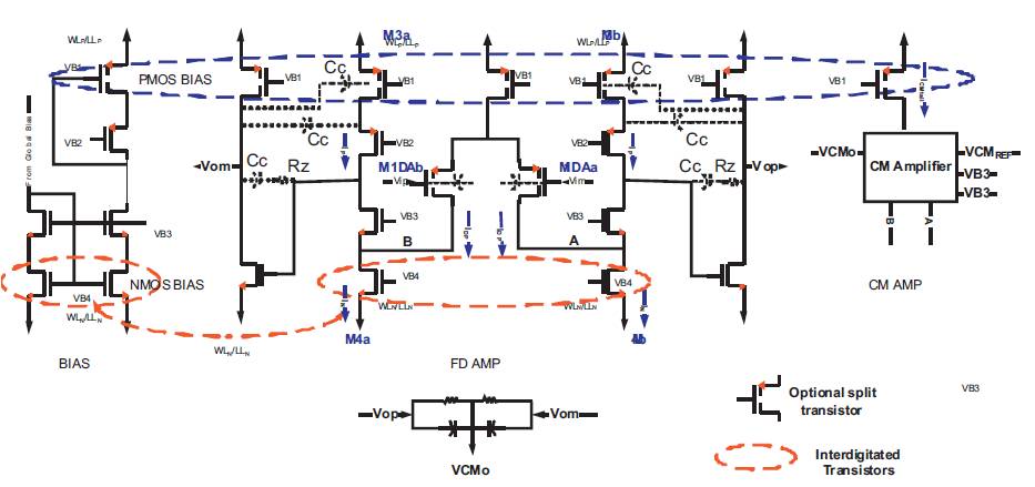
Figure 1. Two stage fully differential OTA (Operational Trans conductance Amplifier) showing transistors interdigitated to improve both common mode and fully differential offset. Well described compensation paths are indicated as well.
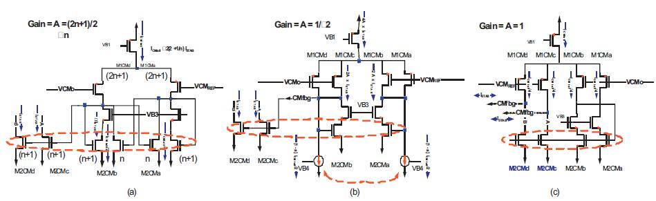
Figure 2. Schematic Diagram of OTA and Common Mode Feedback Circuit of First Stage Amplifier. The NMOS mirrors (c) can be selected as either long channel or signal path devices.
Note that CM tail current mirroring through the CM amplifier establishes I . For Figure 2(c),
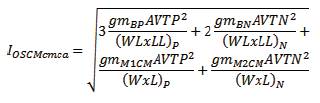
Where for both WL, LL are the long channel device geometries used in the current sources and W, L represents the signal path performance device geometries in both the CM and FD amplifiers. For the CM amplifier of Figure 2(c), modest magnitude variations in the CM tail current have a limited impact on IOSCM which is controlled by matching in the long channel bias transistors in Figure 1. System V is controlled by area and proper layout of the CM amplifier and DC gain, ACM. Effective CM offset voltage is expressed as
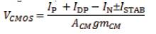
Where ACM , and gmCM , are the voltage gain and transconductance of the CM amplifier respectively. Frequently in high performance applications, the available process of bandwidth or power limit is increasing ACM . The use of the CM amplifier of Figure 2(c) allows the use of only long channel devices to develop primary bias, P and N rail side currents (IP + IDP ) and (IN = IP + IDP ) respectively minimizing current mismatch. Note that when (IP + IDP ) and (IN + ISTAB ) are to match in Figure 2 (a) and (b), ISTAB is mirrored through the CM amplifier with its shorter channel reduced area devices and there will be an increase in error. The CM amplifier of Figure 2 (c) only provides a IOSCM and its VOSCMA is a function of the N and P pair mismatch and to a much lesser of the tail current. The use of longer channel bias current devices improves the FD DC gain, reduces FD and CM offset, and 1/f noise with minimal impact on bandwidth.
To avoid latch up in two stage FD amplifiers when applying Figure 2(a) and (b),ISTAB must be greater than IDP + IP – IN or in the case of the CM amplifier of Figure 2(c) worse case conditions (i.e. start up) allow ISTAB > IDP + IP or< – IN . Latch up is avoided by setting ICMTAIL equal to 2(IDP + IP ) resulting in bounding ISTAB to 2IDP ,when using the CM amplifier of Figure 2, guaranteeing latch up free FD amplifiers under all conditions. With added circuits, CM tail current could be reduced post start up reducing power consumption.
The three CM topologies and their performance are summarized in Figure 2 and Table 1 respectively. All are biased with approximately equal tail currents of 4ISTAB resulting from latch up free and maximum FD bandwidth requirements. CM amplifiers for wide band applications are defined by FD amplifier Gain Bandwidth Products (GBP) approaching one tenth of analog unity current gain bandwidth of the signal path devices or non bias current devices. In general, this dictates that, CM bandwidth must approachTA (gm0 / (L2 Cox)). Typically all signal path transistors TA 0 in such a design are biased near their optimal tranconductance current density (gm0 ) for the desired region of operation, i.e. moderate inversion, or velocity saturation. The more traditional CM amplifier of Figure 2(a) may develop gain and makes identical noise contributions to the FD amplifier as Figure 2(b). Figure 2(b) takes on its more familiar form when ACM equals ½ ( = 1) and bandwidth is TA/2. Of the three configurations, Figure 2(a) has a clear VCMOS offset advantage, but must have the bandwidth headroom and finger area to take advantage. The CM amplifier in Figure 2(c) provides a slight stability advantage under transient conditions but with the potential for added PMOS (PMOS device noise is often notably less than an equivalent NMOS device)via the PMOS differential pair and NMOS noise via long channel mirrors. Table 2 shows the noise contribution by device from a Spectre simulation consisting of an amplifier topology and Figure 2(c) fabricated in an 180nm CMOS process. For the specific process of the simulation, the two stage amplifier input noise is dominated by thermal noise in the long channel rail side NMOS devices (M4a,b) and the CM NMOS devices (M2CMc,d) and PMOS devices of any length are lower noise than their NMOS equivalent. Converting CM amplifier devices, M2DA, to long devices, will reduce their 1/f noise to insignificant levels, leaving only the PMOS differential pair (M2DAa,b) contributing significant 1/f noise.
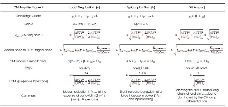
Table 1 Performance metrics for common mode amplifier of Figure 2
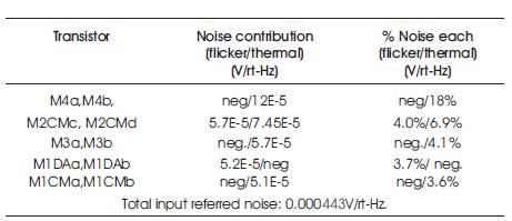
Table 2. Noise Summary For Opamp In ,
The CMCA makes a smaller contribution to rail side current of mismatch than more typical configurations of Figure 2(a) and Figure 2(b) With rail side current mismatch dominated by the long and wide transistors in the bias legs, FD system ICMOS is also less when using CMCA as a result of reduced voltage mirroring errors of the CMCA transistors pairs and first order ICMOS independence from CM tail current (ICMtail ) matching. Finally, by setting the CMCA and FD amplifier differential pairs equal, FD and CM bandwidths can be matched or set independent, with FD and CM compensation tracking across process and temperature. This requires making the NMOS mirrors (M2CM) short channel devices or increasing the CM amplifier gm or tail current. The trade-off is higher power and lower VOSCM and lower 1/f noise or lower power and higher VOSCM and higher 1/f noise. For equal PMOS pairs, CM and FD (equal gms ) amplifiers bandwidths are equal with greater CM phase margin as a result of the reduced CM loading such that.,
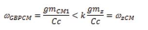
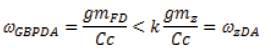
where the non-dominant poles of each are approximately equal [6]. If desired, both CM and FD can be set independently by either adjusting differential pair geometries or using split differential pair compensation [8,9].
An alternate method for developing CM stability has been presented using current mode feedback. All FD amplifier bias currents are set by long wide channel devices, and the differential transconductance currents of Figure 2(c) stabilized the 2-stage FD amplifier phase margin and latch up while reducing VCMOS . Additionally, CM and FD gain bandwidth and phase margin track across process. The CM amplifier of Figure 2(a) can be applied in an identical manner when bandwidth headroom is available, maintaining the previous advantages, while further reducing the common mode VCMOS but with a significant increase in power consumption (proportional to increased gain) when process GBP is available.