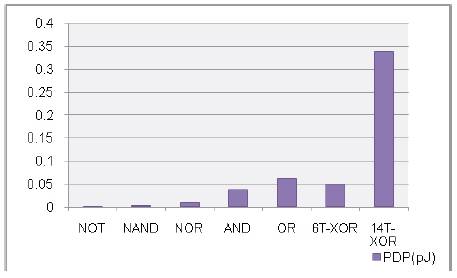
Figure 1. PDP of various logic gates in 45nm technology
Power consumed per unit switching activity in a CMOS based computational unit is greatly dependent on the power consumption of the sum and carry generation units. This paper is focussed on reducing area and PDP of the computational units through gate level and transistor level optimisation. At transistor level 6T Mux based CMOS-CPL XOR gates with stable rise and fall times are used. The concept of gate level Boolean equivalent substitution is used in optimization of logics used in carry generation in a computational unit. Optimised carry block exhibits 50% lesser delay and 45% lesser power consumption compared to a ANDOR based carry generation system. An optimized computational unit at layout level is realised with proposed logical substitutions and with Mux based XOR gates. The resulting computational unit exhibits 60% reduced power consumption compared to a standard realisation. Synthesis of layout and simulations are done by using 45nm technology.
Portable devices demand low power, area efficient computational units for processing and computation. Multiplier is the functional unit in any processor or a computational unit namely an ALU. Multipliers are extensively used in Digital signal processors for performing convolution, correlation and FFT calculations. The speed and the power consumption of a processor is greatly dependent on the speed and power consumption of the multiplier. On the other hand the multipliers are functionally made up of adders [1]. Power consumption and delay of the adders are dependent on the logics used for generation of sum and carry. Area optimisations are dependent on the technology used for fabrication. While power continues to have an inclination towards the logic used in realising a circuit, efforts have been made to reduce the power consumption by reducing the unwanted operation during bit'0' of the multiplier [5]. A low power multiplier is designed in [2], [3]. Optimisation techniques at gate level can reduce the number of gates and there by area and power. So making a wise choice in choice of gates for realising a logic is essential. This paper presents a modified carry generation system with reduced PDP and delay. The low power carry unit combined with Mux based XOR gates are used in realising a low power computational unit that exhibits reduced PDP with no trade-off in delay.
The gate level analysis of various parameters of basic logic gates provides an optimal path for designing a circuit implied for a specific function.The performance parameters such as Power and delay of the various logic gates are estimated and their corresponding PDP's are compared in Figure 1.
Figure 1. PDP of various logic gates in 45nm technology
The CMOS based XOR logic realised using 14 transistors are shown in Figure 2. The CMOS technology has been profoundly used for generating stable outputs with constant high and low times. Here a pre-existing Mux based 6T XOR realisation is compared with CMOS 14T XOR realisation and their corresponding PDP's are shown in Table 1. The Mux based XOR gates are efficient in terms of power, delay and area when compared to CMOS 14T XOR and this can be inferred from Table1. The CPL based Adders [2], [6], [8], [9], [10] suffer from threshold voltage degradation. So using them in cascaded stages may lead to degraded outputs . The threshold voltage degradation is minimum as the output stage of the Mux based XOR, as it employs an inverter. The inputs, output waveforms for CMOS 14T XOR and Mux based 6T XOR are shown in Figure 3 and Figure 5. The PDP comparison of Mux based and 14T XOR gate are shown in Figure1. From Figure 4 and Figure 5 it is evident that the CMOS-CPL based Mux based XOR is power efficient with minimum threshold degradation. So it is chosen as a suitable alternative for CMOS 14T XOR for realisation of efficient computational unit.
The simulated waveforms for CMOS 14T XOR and 6T XOR using 45nm technology with common input patterns and settings are shown in Figure 4 and Figure 5.
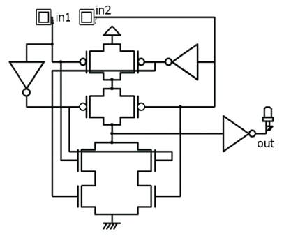
Figure 2. 14 Transistor XOR gate using CMOS technology
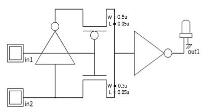
Figure 3. Mux based 6T XOR logic
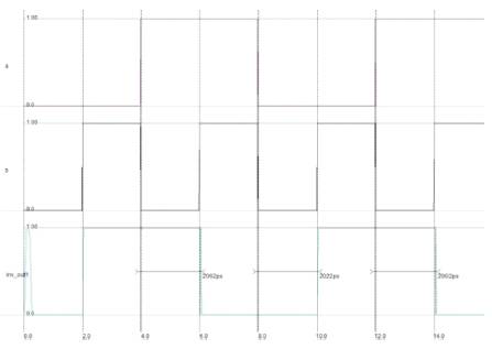
Figure 4. CMOS 14T XOR waveforms
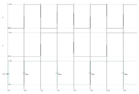
Figure 5. Mux based 6T XOR waveforms
The functions that involves a 3x3 multiplications are shown in Figure 6. Initially partial products are estimated for all levels and the concept of carry save addition is used to propagate the carries obtained at level "i" to the next column to the left in the level "i+1". Figure 6 shows a 3x3 multiplication and the various steps involved.
The concept of carry save addition is inherently used in high speed multiplication. Concept involves propagation of carry obtained at various levels to the final level where they are added by the mechanism of carry look ahead addition and here P5 term in the product obtained is the final carry and it occupies the MSB of the product term. The gate level architecture of a 3x3 multiplier is shown in Figure 7, The gate level structure is realised using logical AND, logical OR and logical XOR gates.
The gate level optimization is a high level optimization in which a group of gates with equivalent Boolean functions [7] can be substituted in the place of one another for realization of circuits implied for Specific applications. A function involving two logical AND and logical OR are shown in Figure 7. An equivalent logic of Figure 7 is shown in Figure 8. Analysis of both the structures at gate level show a reduction in PDP, in the realization based on NAND gates and also the logical realisation as shown in Figure 8 exhibiting low area when compared to the logical realisation shown in Figure 7.
Equations of carry can be written as
let in1=A, in2=B, in3=C, in4=A^B in the logical realisation shown in Figure 7 and Figure 8. respectively
Now output of the logic shown in Figure 7 will be
Now output at Gate1 from Figure 8.

Now output at Gate2 from Figure 8.
Now output at Gate 3 from Figure 8.
From DEMORGANS Law [7]
Applying equation(6) on (5) equation (5) can be written a
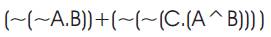
Equation (7) can be written as
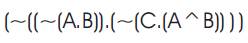
Hence from the Equations (2),(7),(8) the logical realisation shown in Figure 7 and Figure 8 are equivalent. Thus the logic shown in Figure 7 can be substituted with the logic showed in Figure 8. (note the functional symbols ~ NOT,. AND, + OR) The NAND based system for the carry Generation offers savings in the number of transistors needed for implementation by 7 transistors which will amount to 45 % savings in the number of transistors used and it offers 50%savings in power compared to an ANDOR logic, as shown in Table 1.
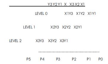
Figure 6. The various steps involved in 3 x 3 multiplications
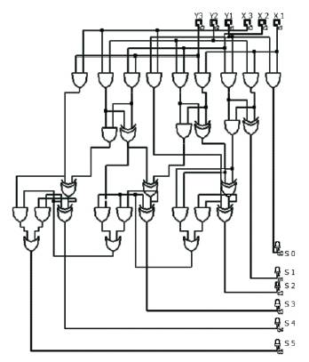
Figure 7. Gate level realisation of a 3 x 3 multiplier
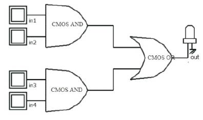
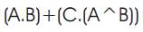
Figure 8. Boolean function (in1.in2) + (in3.in4) using and ANDOR gates
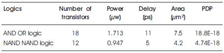
Table 1. Performance And Physical Parameters of Carry Generation Units
The proposed modification for power reduction involves logical substitution of the logics involving ANDOR with proposed NAND based logic and the use of Mux based XOR logics. The computational unit uses carry save addition for generation of the final carry that occupies the MSB in a product term. The proposed architecture is found to be efficient in terms of area and power when compared to unoptimized logic and shows reduced PDP and Reduced area. The gate level architecture of the proposed multiplier is shown in Figure 10. A reduction of 2 transistors per gate can be achieved in the carry generation unit and this will amount to larger number of transistors reduced when a larger multiplier is considered. AND gates in CMOS logic are formed from NAND gates and OR gates are formed from NOR gates by connecting an inverter to the corresponding NOR. Hence the use of pure NAND based logics offers savings in metal layers and contact vias needed for Connecting Vdd and Gnd and inputs and outputs in additional inverter stages found in AND and OR gates. An ASIC implementation of a high performance multiplier is given in [4]. Layout of the optimised multiplier designed is shown in Figure 12. The architecture of the optimised multiplier is given in Figure 9.
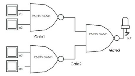
Figure 9. Boolean function (in1.in2 )+ (in3.in4) using 3 NAND gates
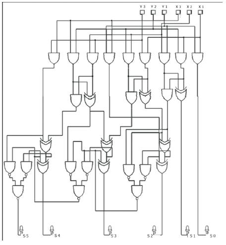
Figure 10. Gate level architecture of proposed multiplier for 3 x 3 multiplication
The layout level analysis of the CMOS 14T XOR based multiplier is done and the corresponding waveforms obtained are shown in Figure 11, The analysis is done with common input patterns and setup using 45nm technology.
The layout level analysis shows that the realisation based on CMOS 14T XOR consumes more power, area and has an increased PDP compared to the realisations that use 6T XOR logic, The comparisons are shown in Table 2.
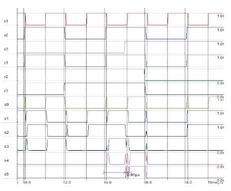
Figure 11. Output waveforms for CMOS XOR based multiplier
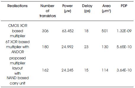
Table 2. Performance And Physical Parameters of Computational Units
The layout level analysis of the 6T XOR based multiplier with ANDOR logic for carry generation is done and the corresponding waveforms obtained are shown in Figure12, The analysis is done with common input patterns and setup using 45nm technology.
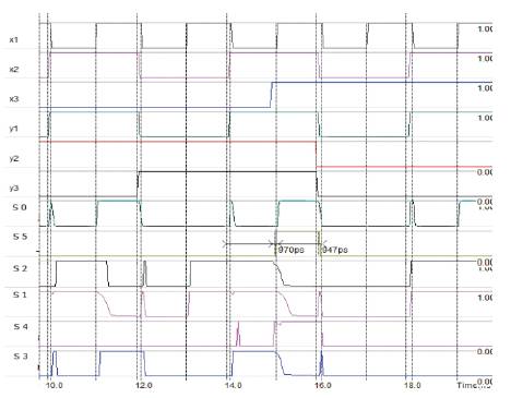
Figure 12. Waveforms for 6T XOR based multiplier
The layout level analysis of the 6T XOR based multiplier with proposed NAND based carry generation logic is done and the corresponding waveforms obtained are shown in Figure14. The layout of the multiplier based on proposed and suggested logical optimisations is obtained using 45nm technology and it is shown in Figure13.
Number of metal layers and contact vias in NAND based carry unit when compared with ANDOR is lesser. This reduces the overall load capacitance. The reduction in capacitance reduces the delay. The computational unit based on NAND based carry unit and Mux based XOR gates has a reduced PDP when compared with other realisations with ANDOR carry unit. The power consumption of the optimised layout proposed is 60% lesser than the realisation without optimisation.
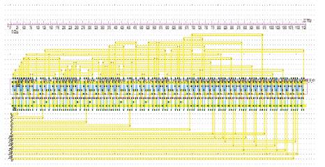
Figure 13. Layout of the proposed 3 x 3 multiplier
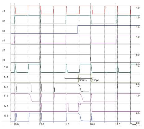
Figure 14. Waveforms for proposed multiplier
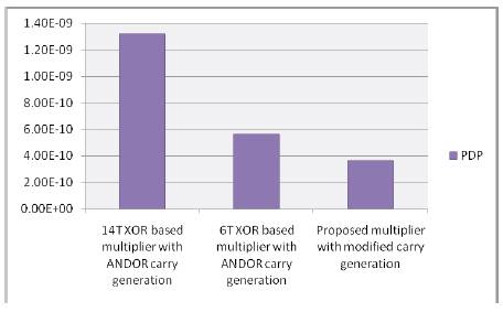
Figure 15. Graph showing the variation of PDP among different realizations of computational unit
From Table 2 and Figure13 it is evident that gate level optimisation by means of Boolean equivalent substitution and use of 6T based Mux based XOR gates holds good for high performance circuit realisations and the proposed optimised multiplier layout for 3 x 3 multiplication has a minimal area of 114µm² with 162 transistors which is 48% lesser when compared to the realisation based on CMOS XOR and ANDOR based carry unit. The proposed optimised multiplier layout shows a reduction of power consumption of by 60% and shows considerable reduction in PDP by 70% when compared with a realisation without optimisation as shown in Table 2. Thus the NAND logic based carry generation system favours reduction in delay and power consumption reducing the PDP of the functional unit.