(1)
As the feature size shrinks, Electromigration (EM) becomes a more critical reliability issue in IC design. EM around the via structures account for much of the reliability problems in ICs [13]. Electromigration is increasingly relevant to physical design of the electronic circuits. It is caused by excess current density stress in the interconnect. The ongoing reduction of the circuit feature sizes has aggravated the problem over last couple of years. It is therefore an important reliability issue to consider electromigration-related design parameters during physical design as life-span of the chip is defined by how well EM verification is done for that chip. So EM is a very important check to be taken care in reliability checks. Literature deals with different aspect of EM in [1], [2], [10], [21], and [22], . In this paper, an effort is made to review different aspects of EM, solution proposed and scope for improvement. The authors have reviewed and identified various fascinating issues and possible solutions to address them.
Technology scaling has traditionally offered advantages to embedded system design in terms of reduced energy consumption, cost, and increased performance. Scaling past the 45 nm technology node however, brings a host of problems, whose impact on system-level design has not been evaluated rigorously. Random intra-die process variability, reliability, and their combined impact on the system level parametric quality metrics are effects that are gaining prominence. Dealing with these new challenges require a paradigm shift in the system level design phase. The dominating reliability issues in the lower technology is Electromigration [18].
Electromigration (EM) reliability is becoming a serious problem for integrated circuit due to feature size shrinking. Interconnects, especially via's, in Power/Ground (P/G) network suffer from significant EM degradation as they carry large current. The EM effect on P/G via's, considering uneven current distribution in via array and time-varying current loads [16].
There are different parameters related to EM. The parameters related to ElectroMigration process are described as follows.
In [9], Current flow through a conductor produces two forces to which the individual metal ions in the conductor are exposed. The first is an electrostatic force F caused field by the electric field strength in the metallic interconnect. Since the positive metal ions are to some extent shielded by the negative electrons in the conductor, this force can be ignored in most cases. The second force F is wind generated by the momentum transfer between conduction electrons and metal ions in the crystal lattice. This force works in the direction of the current flow and is the main cause of electromigration[9], [10].
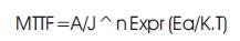
Many electronic interconnects, for example in integrated circuits, have an intended MTTF (Mean Time To Failure) of at least 10 years. The failure of a single interconnect caused by electromigration can result in the failure of the entire circuit. At the end of the 1960s the physicist J. R. Black developed an empirical model to estimate the MTTF of a wire, taking electromigration into consideration [2], [10]:
Where A is a constant based on the cross-sectional area of the Interconnect, J is the current density, Ea is the activation energy (e.g. 0.7 eV for grain boundary diffusion in aluminium), k is the Boltzmann constant, T is the temperature, and n is a scaling factor (usually set to 2 according to Black). It is clear that current density J and temperature T are deciding factors in the design process that affect electromigration [5].
In [15], Current flow in a wire causes Joule heating, which has tens EM, as seen in equation (1) is shown. The temperature T in a wire is given by,
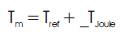
where T is the reference chip temperature for EM analysis ref and _T is the temperature rise due to Joule heating[10].
It is known that pure copper used for Cu-metallization is more electromigration-robust than aluminium. Copper wires can withstand approximately five times more cur-rent density than aluminium wires while assuming similar reliability requirements. This is mainly due to the higher electromigration activation energy levels of cop-per caused by its superior electrical and thermal con-ductivity as well as its higher melting point [9], [12].
In equation (1), the temperature of the conductor appears in the exponent, i.e. it strongly affects the MTTF of interconnect. The temperature of interconnect is mainly a result of the chip environment temperature, the selfheating effect of the current flow, the heat of the neighbouring interconnects or transistors, and the thermal conductivity of the surrounding materials [6], [9], [19].
As equation (1) shows, apart from the temperature, it is the current density that constitutes the main parameter affecting the MTTF of a wire. Since the current density is obtained as the ratio of current I and cross-sectional area A, and since most process technologies assume a constant thickness of the printed interconnects, it is the wire width that exerts a direct influence on current density [4] the wider the wire, the smaller the current density, and the greater the resistance to electromigration. However, there is an exception to this accepted knowledge: If you reduce wire width to below the average grain size of the wire material, the resistance to electromigration increases, despite an increase in current density.
Reliability and Electromigration effect on deep sub-micron technology are studied and reviewed from recent research publications. The relevant issues and methodologies are discussed by these articles are reviewed in this paper. The current trends and future scope of activities is outlined in the conclusion.
The ongoing reduction of circuit feature sizes has aggravated the EM problem over the last couple of years. It is therefore an important reliability issue to consider Electromigration-related design parameters during physical design [9], [10], [12].
Electromigration-aware physical design flow is proposed (Figure 1) to take care of the above problem.
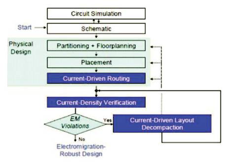
Figure 1. Electromigration-aware Physical Design Flow [9]
In order to address EM problem, this paper has focused on basic design issues that affect Electromigration during interconnect physical design. Here, most measures aim at limiting the current densities in all parts of the circuits, notably interconnect and terminal connections [11].
Finally, an Electromigration-aware physical design flow. In addition to the regular design steps, this flow contains three current-density-driven design and verification tools which allow an effective consideration of electromigrationrelated constraints during physical design.
Authors in [2] and [7] present a design strategy using Special Signal Non-Default Routing Rules (SSNDRs) to re-route the wire segments of critical nets that present a high current density and are EM unsafe. Some EM-aware design steps are added in the traditional design flow to analyze, fix and improve the Mean Time to Failure (MTTF) of the designs[9].
In order to improve the current distribution, they have tested some Special Signal Non Default Rules (SSNDRs) applied to the critical signal nets into the design. Once we identify the critical nets, the SSNDRs are set on cadence EDI. The routing rule for the violated wire segments is applied. Then, the AC analysis is re-executed to check if the violation is clean. This flow can be repeated as many times as it is needed. When there are no violations and a DRC clean design, the process is stopped and the MTTF is reanalysed to analyse the effective improvement given by the SSNDRs flow.
They have also presented a case study that highlight this issue in a 22 nm technology node. They have presented a customized EM-aware design flow to improve the circuit lifetime by changing specific wire segments to reduce the current density that causes EM reducing the circuit MTTF.
The papers [13], [21] address the impacts of via configuration on electromigration from both physical and statistical point of view.
A series of test structures with different via arrangement o (Figure 3) are tested at 325 C at a current density of 5 2 MA/cm in the conductor line in series with via configurations. All sample consisted of a conductor line with 0.186 um in line width and 150 um in length. This will provide straight forward comparison between different via structures and eliminate possible design variations, including via/trench aspect ratio, thickness, etc.
In summary simply using either a redundant or large via does not improve the life time of all the testing structures they stressed. However, the sigma value improves quite significantly in the distribution. For the case of via's along the length in the direction of current flow, it is remarkable how well it helps to alleviate the impact of early fails. Other hand, it might generate a false sense of security if small via is replaced with large one to improve the overall EM reliability.
The papers [1] and [3] compare the EM results derived from novel and traditional test structures, a new EM failure mechanism is also proposed. The new mechanism is caused by the Cu/barrier interface damage at the metal line-edge during upper via opening process. This damage provides a fast diffusion path. From the downstream EM test (Figure 4), it is observed that the thicker Ta-based ALD barrier has a higher activation energy and median time to failure compared to thinner Ta based barrier. Thicker barrier process enhances Cu/barrier adhesion and hence prevent the via opening induced interface damage.
Besides the traditional one-directional upstream and downstream EM tests, four kinds of current stress paths were applied to the novel structure during EM characterization in Figure 2, i.e. two downstream paths with (1) from pad-B to pad-C and (2) from pad-B to pad-D and two upstream paths (3) from pad-A to pad-C and (4) from pad-A to pad-D.
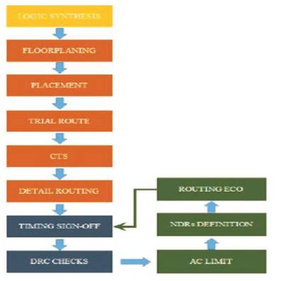
Figure 2. SSNDR Optimization within Design Flow [2]
Figure 3. Top Down View on Different Via Configuration [19]
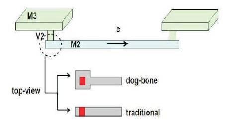
Figure 4. A Dog-bone Structure with Large Metal Enclose of via to Prevent via Landing on Metal Line Edge at Line Ends Compared to Traditional Downstream Structure [1]
Process scaling will push for thinner metal barrier, while thinner Ta-based ALD barrier will cause a new failure mechanism. A novel EM test structure has been designed as shown in Figure 5 to verify the new failure mechanism that via opening process may induce Cu/barrier interface damage on metal line edge. Through barrier process improvement, one can find optimized barrier thickness with a reliable Cu/barrier adhesion and still meet circuit requirement.
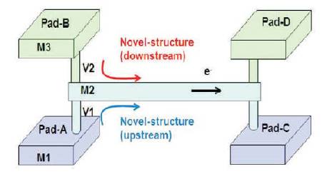
Figure 5. A Novel EM Reliability Test Structure Design which Combines Downstream and Upstream [1]
Short length effect on Electromigration (EM) of 40 nm Low-k Cu interconnects was investigated through downstream structure and via chain. It is found that EM Mean Time-To- Failure (MTTF) of short length metal can be enhanced at least 20 times. It is also observed that EM performance of short metal length degrades much slower, which can be applied to improve interconnect EM performance through via chain made of short length metal [14], [22].
EM TTF lognormal distribution of short length metal was investigated to show the short length effect on EM performance based on 40 nm technology node. It is found that short length has a significant improvement effect on EM performance. Besides, it is found that EM TTF of short length metal degrades much slower than normal length metal. Short length's effect on improving EM performance through via chain is also discussed [8], [17], [20].
Via 1 downstream (V1D) and Via 2 downstream (V2D), and via chain were selected to evaluate the short length effect of metal line on EM performance as shown in the Figures 7 and 8.
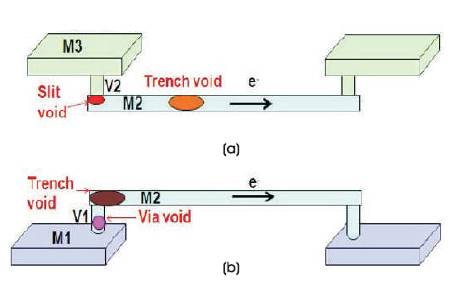
Figure 6. Traditional EM Reliability Test Structure and Failure Mode for (a) Downstream (b) Upstream [1]
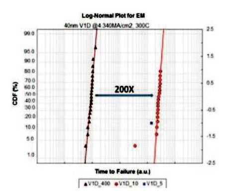
Figure 7. EM TTF lognormal Distribution of V1D from different Metal Length based on 40 nm [20]
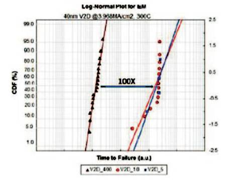
Figure 8. EM TTF lognormal Distribution of V2D from different Metal Length based on 40 nm [20]
Short length effect was explored on downstream EM structure and via chain based on 40 nm technology node [22]. It is found that short length effect can enhance EM MTTF at least 20 times compared with that of normal length metal. Besides, it is also observed that short length effect degrades lognormal TTF distribution much slower. This can be verified through via chain made of short length metal, which behaves perfect EM performance to improve interconnect reliability.
Different research publications that have been reviewed have addressed the following problem related to EM.
These researchers analyze about how to improve mean time to failure using various methods like design parameters, via configuration, thicker copper material, and making device shorter in length. However, they do not address the major issue that VLSI industry is facing right now, is "EM tool run time". This problem is critical since size of the design grows when the number of transistors in IC increases exponentially.
As the technology is scaling down, the number of gates per chip has increased. This internally increases size of the design blocks used in the chip. When we run the EM on the bigger blocks, it takes more time to run with current industry standard EM tool (Cadence VPS, Apache Totem, SigEM, etc). As EM is an iterative process, to clean the EM for bigger blocks it takes lot of time. It is important to improve run time for EM tool to take care of the industry needs.
A new methodology is required to address the major problem that industry EM tools are facing right now, i.e. run time. Electromigration check will be run at last stage of VLSI design steps. Layout designer will have lesser time to verify EM issues along with other reliability checks like IR, antenna, etc.
It is important to have EM methodology to verify EM issues faster, so that it helps the layout designer for fast reliability checks. The new methodology for EM tool should improve run time by maintaining the accuracy. Taking care of accuracy along with run time is a very critical aspect for EM closer. It should check reliability issues in all process corners and in wide temperature range. Option for faster revalidation after fixing reliability issues should be considered.
Authors believe that the consideration of runt time and accuracy should be an integral part of any future EM methodology development.