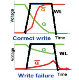
Figure 1. SRAM Cell Write Operation
The increased effect of process variation and increase in parasitic resistance and capacitance in nano scale technologies at lower supply voltages, and continuous increase in the size of SRAMs require additional techniques, such as write assist and read assist to improve the write-ability, readability, and stability of SRAM memories. The SRAM bit cell write-ability is very critical at lower voltages. The impact of the write assist technique is analysed in this paper which will improve the write-ability of the SRAM memory and also its impact on the performance, power, and area of the chip. The Negative Bit-line Voltage Bias scheme is discussed and executed at the transistor level using conventional SRAM cell (6T). With the write assist circuit, the implemented SRAM bit cell efficiently performs a write operation at lower voltages. The main objective of this paper is to improve the write-ability of the SRAM cell at lower supply voltage using Negative Bit-line Write Assist Circuit.
Moore's law motivates the technology scaling in order to improve the performance features, such as speed, power consumption, and area. The power consumption is a major concern in VLSI chip design of a battery operated system [1]. SRAM plays a critical role and consumes a significant amount of power in almost every SoC. With ever increasing scaling of integration, power consumption becomes a challenging problem in modern Integrated Circuit design. As a key tactic toward power saving, Nearthreshold SRAM design has been widely used in SoC design. Lowering the supply voltage is the quadratic effect on the dynamic energy power consumption. However, down scaling on the supply voltage and terrible logic delay can significantly degrade the write ability of a Nearthreshold SRAM design. Process variation effects, such as variation in critical dimensions (W and L), and oxide thickness (T ) also lead to decrease in the write-ability and ox stability of the SRAM cell. Therefore, write assist circuits are needed to improve the design robustness at lower voltages.
This paper is organized as follows. Section 1 explains the write failures in the SRAM design and section 2 discusses the proposed write assist circuit technique. Section 3 presents the simulation results carried out using the Cadence simulation tool and finally the paper is concluded.
Write-ability failure occurs when the internal node voltage – (Q, Q in Figure 3 does not reach to the desired voltage level as shown in Figure 1). To improve the write-ability of SRAM memory, several write assist techniques have been suggested [2]. These assist techniques are cell VDD collapse [weaker pull-up device] [6], boosted word- line voltage [stronger access devices], Negative bit line voltage [stronger access devices without boosting the word line voltage] [3], and raised cell ground [weaker pullup device]. The boosted word-line voltage technique increases the word line voltage connected to the gate of pass/access transistors during write operation. This increases the V (Gate Source Voltage) of access transistors gs and improves its driveability. Cell VDD collapses and raised cell ground techniques reduce the current to the pull-up PMOS device. As a result, it improves the write ability of the cell by weakening the back to back inverters during write operation [4]. However, these techniques worse the hold static noise margin of the half-selected cells and does not meet the requirements for low voltage applications. Among the existing techniques, negative bit line write assist technique is the most effective one to decrease SRAM minimum supply voltage.
Figure 1. SRAM Cell Write Operation
The six transistor SRAM cell with write assist circuit is shown in Figure 2. This circuit splits into three distinct parts. The conventional 6T SRAM cell structure is shown in Figure 3. It is composed of two cross-coupled inverters (M1-M4) with two access transistors (M5, M6) connected to complementary bit-lines (BL, BLB). Both access transistors are connected to the Word Line (WL) to perform the access write and read operations through the bit lines. In write mode, initially both the bit-lines will be pre-charged to supply voltage VDD. One of the bit- lines will be driven to low through a write driver. Then, with WL, the data held high on bit-line will be written to the internal storage node of the SRAM bit cell.
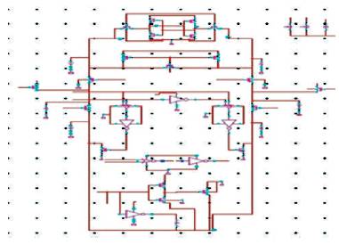
Figure 2. SRAM Memory Cell with Write Assist Technique
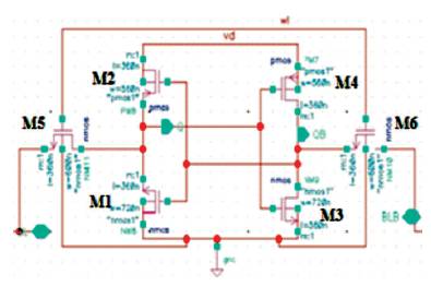
Figure 3. Conventional 6T SRAM Cell
In read mode too the bit-lines are initially pre-charged to VDD. Then when the word-line is selected, (VDD) bit-line discharges via M6 and M3 (node Q=0), so that differential voltage develops across the bit-lines [5]. This differential voltage should be large enough for a sense amplifier to detect the state of the cell. Secondly, the pre-charge circuit, helps the pre-charging of bit lines. The Negative bit line voltage write assist circuit is shown in Figure 4, which helps to improve the write-ability of the SRAM memory.
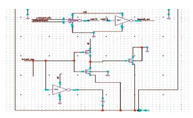
Figure 4. Negative Bit Line Voltage Circuit
One of the best write assist circuit techniques to improve the SRAM cell write-ability is Negative Bit-line Scheme. The principle behind this approach is that, bit line voltage is pulled into negative (below ground potential), which will increase the strength (V ) of the access transistor [8] . With gs increased V , the access/pass transistor will discharge the gs cell node “1” below the V of the cross-coupled PMOS of tp the SRAM latch, which ensures proper write operation of the bit cell. For low power supply applications, the conventional SRAM memory couldn't complete the write operation within the specified word line pulse width due to the lower V or lower drive-ability on pass transistor.
The proposed Negative bit line voltage write assist circuit scheme will help the write operation at reduced word line pulse width at lower power supply. Figure 4 shows the negative bit line technique for expanding the write margin. Making use of a self-determining circuitry as for the BL and/BL, it is essential to adjust the timing of forcing one of them to a negative bias. It includes boost_en circuit, one boosting capacitor C , connected to bit-lines BL and BLB, boost and inverter circuit. The boost_en signal is generated based on pre-charge (prech), which is properly synchronized with Word-Line signal (WL), Write Enable (WE), and column select (CSELECT) signals. The NBL voltage circuit will generate the negative bias and it will couple the negative voltage to the bit line, whichever is discharging thereby it pulls the bit line voltage to a negative level [7]. The amount of negative voltage level on bit line depends on the Boost Capacitance (C ) vs. Bit Line Capacitance boost (C ). More the bit line capacitance less will be the negative BL boost level. Similarly, more the boost capacitance, higher the negative billion levels.
Therefore negative bit line voltage level depends on the ratio of C / (C +C ).
This negative bit line voltage helps for the faster discharge of the SRAM cell node “1” and improves the write-ability operation. It is necessary to ensure that the negative bit line voltage level should not create any false write operation on the half-selected bit cells . Also the negative bit line level should not create any reliability issues for the access transistor due to higher V [9]. If the boost_en signal is low, gs the write assist circuit is disabled and both the bit lines are connected to the predefined voltage level of VDD, and at this mode SRAM will perform the normal operation.
Stability and performance are the key parameters of SRAM design. Hence, both, conventional 6T and negative bit line write assist circuit SRAM cells have been analysed for these parameters. Figure 5 shows simulation result of the unsuccessful write operation of the SRAM bit cell when write assist circuit is not used at lower power supply voltage (0.72 V). It explains the need of the negative bit line assist circuit for the proper write operation of the SRAM memory at lower voltages.
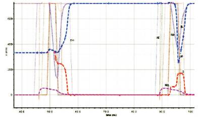
Figure 5. Unsuccessful Write Operation without Assist Technique
The boost_en enable signal is asserted when the bit line is discharged close to zero (ground) potential. Depending on the Boost capacitance vs. bit line capacitance values, the bit line is pulled to the negative voltage. It is observed that even at -75 mV on the bit-line, the memory shows a successful write operation at 0.72 V as shown in Figure 6. Without this negative boost on bit line write operation failed. It shows the significance of the write assist technique at lower supply voltages. The advantage and impacts of the proposed write assist technique on performance and power are explained in Table 1. The power consumption and delay are observed, which shows performance has been improved and average power increases during write operation and also it results in increase of leakage.
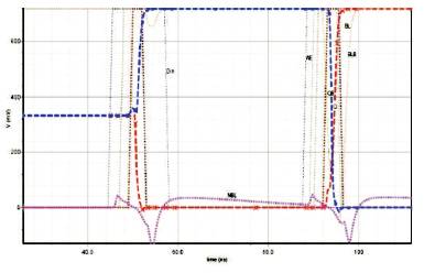
Figure 6. Successful Write Operation using Assist Technique
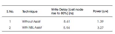
Table 1. Performance and Power Calculation of SRAM with and without Assist Circuit
In this paper, the authors have proposed a write assist scheme for generating negative bit line voltage at lower supply voltages for proper write operation. Negative bit line scheme can achieve higher reduction in write failures compared to lower cell supply voltage while preserving the benefits of bit-line (or column) based control (in fact halfselect stability improves marginally) and eliminating the need for additional voltage levels. Hence, the negative bit line scheme can be very helpful in lower supply voltages and robust SRAM design under process variation in nanometre technologies. The advantage and impacts of the proposed write assist technique on performance and power are explained.
To improve the operating voltage range of SRAM memory arrays in the presence of PVT (Process, Voltage, and Temperature) variations, various circuit assist techniques have been developed. Among all the write assist techniques, the authors recommend that the proposed negative bit line write assist technique gives the optimized circuit at lower supply voltages. However, forcing one of the bit lines to negative voltage, a non-zero V will appear gs across the access transistors of un-accessed rows. This can lead the cell to flip, causing a write stability error. So, the excessive negative voltage on bit line will cause the stability of the SRAM cell..