Figure 1. CAM Block Diagram
The design of high speed Content Addressable Memory (CAM) offers high speed search function in a single clock cycle. Content addressable memory is a memory that implements the lookup-table function in a single clock cycle using dedicated comparison circuitry. In the CAM, design techniques are at the circuit level and at the architectural level. At the circuit level, low-power match-line sensing techniques and search line driving approaches are utilized. In the existing system, a parity bit has been that leads to introduced sensing of delay reduction at a cost of less than area and power overhead. Thus robust, high-speed and low-power match line sense amplifiers are highly sought in CAM designs. In the proposed system, a double parity bit is introduced for searching data, and thus speed and power is increased. Without sacrificing speed, power is reduced by using gated clock technique.
Most memory devices store and retrieve data by addressing specific memory locations. As a result, this path often becomes the limiting factor for systems that rely on fast memory accesses. The time required to find an item stored in memory can be reduced considerably if the item can be identified for access by its content rather than by its address. A memory that is accessed in this way is called Content-Addressable Memory or CAM (Content Addressable Memory). CAM provides a performance advantage over other memory search algorithms, such as binary or tree-based searches or look-aside tag buffers, by comparing the desired information against the entire list of pre-stored entries simultaneously, often resulting in an order-of-magnitude reduction in the search time.
CAM is ideally suited for several functions, including Ethernet address lookup, data compression, patternrecognition, cache tags, high-bandwidth address filtering, and fast lookup of routing, user privilege, security or encryption information on a packet-by-packet basis for high-performance data switches, firewalls, bridges and routers. This paper discusses on several of these applications as well as hardware options for using CAM.
Since CAM is an outgrowth of Random Access Memory (RAM) technology, in order to understand CAM, it helps to contrast it with RAM. A RAM is an integrated circuit that stores data temporarily. Data is stored in a RAM at a particular location, called an address. In a RAM, the user supplies the address, and gets back the data. The number of address line limits the depth of a memory using RAM, but the width of the memory can be extended as far as desired. With CAM, the user supplies the data and gets back the address. The CAM searches through the memory in one clock cycle and returns the address where the data is found. The CAM can be preloaded at device start-up and also be rewritten during device operation. Because the CAM does not need address lines to find data, the depth of a memory system using CAM can be extended as far as desired, but the width is limited by the physical size of the memory.One of the key design challenges of today's high-capacity CAMs is reducing power consumption. The high power consumption of CAMs is due to the parallel nature of the CAM search operation in which a large amount of circuitry is active on every cycle. Since the power consumption of CAMs is proportional to the CAM memory size, CAM power consumptions increase as applications require larger CAM sizes.
Power gating is a technique used in integrated circuit design to reduce power consumption, by shutting off the current to blocks of the circuit that are not in use. In addition to reducing stand-by or leakage power, power gating has the benefit of enable condition. Clock gating is a popular technique used in many synchronous circuits for reducing dynamic power dissipation.
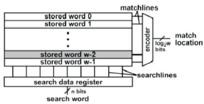
In general, a Content Addressable Memory (CAM) has three operation modes: READ, WRITE, and COMPARE, among which "COMPARE" is the main operation as CAM rarely reads or writes. It starts a compare operation by loading an n-bit input search word into the search data register. The search data are then broadcasted into the memory banks through n pairs of complementary Search-Lines (SLs) and directly compared with every bit of the stored words using comparison circuits. CAM can be used to accelerate any applications ranging from localarea networks, database management, file-storage management, pattern recognition, artificial intelligence, fully associative and processor-specific cache memories, and disk cache memories. Figure 1 shows the block diagram of CAM.
Figure 1. CAM Block Diagram
The full parallel search operation leads to critical challenges in designing a low-power system for highspeed high-capacity CAMs. The power hungry nature due to the high switching activity of the SLs and the MLs and a huge surge-on current (i.e., peak current) occurs at the beginning of the search operation due to the concurrent evaluation of the MLs which may cause a serious IR drop on the power grid, thus affecting the operational reliability of the chip. As a result, numerous efforts have been put forth to reduce both the peak and the total dynamic power consumption of the CAMs . For example, [1] and [2] introduced selective pre-charge and pipe-line architecture respectively, to reduce the peak and average power consumption of the CAM utilized in the ML pre-charge low scheme (i.e., low ML swing) to reduce the average power consumption. These designs however, are sensitive to process and supply voltage variations. The tag portion of a cache compares its input, which is an address, to all addresses stored in the tag memory. In the case of match, a single match line goes high, indicating the location of a match. Unlike CAMs, caches do not use priority encoders since only a single match occurs; instead, the match line directly activates a read of the data portion of the cache associated with the matching tag.
Each stored word has a match line(ML) that is shared between its bits to convey the comparison result. Location of the matched word will be identified by an output encoder, as shown in Figure 2. During a pre-charge stage, the MLs are held at ground voltage level while both SL and ~SL are at Vdd. During evaluation stage, complementary search data is broadcasted to the SLs and ~SLs. When a mismatch occurs in any CAM cell (for example at the first cell of the row D= "1"; ~D= "0"; S= "1";~S= "0"), transistor P3 and P4 will be turned on, charging up the ML to a higher voltage level.
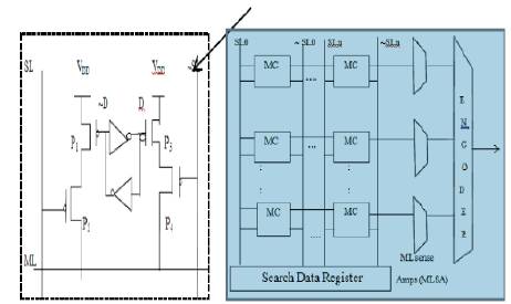
Figure 2. Block Diagram of a Conventional CAM
A sense amplifier (MLSA) is used to detect the voltage change on the ML and amplifies it to a full CMOS voltage output. If mismatch happens to none of the cells on a row, no charge up path will be formed and the voltage on the ML will remain unchanged, indicating a match [3].
A newly introduced auxiliary bit at a glance is similar to the existing Pre-computation schemes but in fact has a different operating principle. Firstly the Pre-computation schemes can be discussed before presenting the proposed auxiliary bit scheme.
The pre-computation CAM uses additional bits to filter some mismatched CAM words before the actual comparison. These extra bits are derived from the data bits and are used at the first comparison stage. For number of "1" the stored words are counted and kept in the Counting bits segment. When a search operation starts, number of "1"s in the search word is counted and stored to the segment on the left . These extra information are compared first and only those that have the same number of "1"s (e.g., the second and the fourth) are turned on in the second sensing stage for further comparison as shown in Figure 3. This scheme reduces a significant amount of power required for data comparison, statistically. The main design idea is to use additional silicon area and search delay to reduce energy consumption.
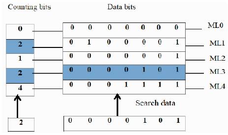
Figure 3. Conceptual view of Conventional Pre-Computation CAM
The previously mentioned pre-computation and all other existing designs share one similar property. The ML sense amplifier essentially has to distinguish between the matched ML and the 1-mismatch ML. This makes CAM designs sooner or later face challenges since the driving strength of the single turned-on path is getting weaker after each process generation while the leakage is getting stronger. This problem is usually referred to a Ion/Ioff . Thus, we propose a new auxiliary bit that can concurrently boost the sensing speed of the ML and at the same time improve the Ion/Ioff of the CAM by two times.
The parity bit based CAM design is shown in Figure 4 consisting of the original data segment and an extra onebit segment, derived from the actual data bits. We only obtain the parity bit, i.e., odd or even number of "1"s. The obtained parity bit is placed directly to the corresponding word and ML. Thus the new architecture has the same interface as the conventional CAM with one extra bit. During the search operation, there is only one single stage as in conventional CAM. Hence, the use of this parity bits does not improve the power performance. However, this additional parity bit in theory, reduces the sensing delay and boosts the driving strength of the 1-mismatch case (which is the worst case) by half, as discussed below.
In the case of a match in the data segment (e.g., ML3), the parity bits of the search and the stored word is the same and thus the overall word returns a match. When 1 mismatch occurs in the data segment (e.g., ML2), number of "1"s in the stored and search word must be different by 1. As a result, the corresponding parity bits are different. Therefore now we have two mismatches [4] (one from the parity bit and one from the data bits) shown in Figure 4. If there are two mismatches in the data segment (e.g., ML0, ML1 or ML4), the parity bits are the same and overall we have two mismatches.
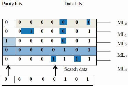
Figure 4. Conceptual view of proposed parity-bit based CAM
With more mismatches, we can ignore these cases as they are not crucial cases. The sense amplifier now only have to identify between the 2-mismatch cases and the matched cases. Since the driving capability of the 2- mismatch word is twice as strong as that of the 1- mismatch word, the proposed design greatly improves the search speed and the Ion/Ioff ratio of the design.
A parity-bit is introduced to boost the search speed of the parallel CAM with less power and area overhead. Concurrently, a power-gated ML sense amplifier is proposed to improve the performance of the CAM ML comparison in terms of power and robustness [6].
In the double parity bit, the searching elements are the parity bits. In this one parity bit is for MSB and another parity bit is for LSB. Normally, the searching elements are used for finding the address location of the data stored. Here, we have taken eight bit data and that data bit is search data against the stored data(Data bits). In the above parity bit based cam single parity was used, now we are using double parity bits.
In double parity with weightage, weightage is a searching element, Weightage means Most Significant Bit(MSB) and Least Significant Bit(LSB). Previously, by using double parity bit, searching speed increases and the weightage is used to compare the stored data bit easily. While comparing MSB and LSB, if MSB is greater than LSB, then weightage is one, if MSB less than LSB means than weightage is zero and when MSB is greater than or equal to LSB, means the priority is taken as (MSB > LSB) one.
The proposed CAM architecture is depicted in Figure 5. The CAM cells are organized into rows (word) and columns (bit). Each cell has the same number of transistors as the conventional P-type NOR CAM and use a similar structure. The gated-power transistor is controlled by a feedback loop, denoted as "Power Control" which will automatically turn off the transistor [5].
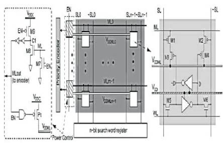
Figure 5. Power gated CAM
Clock signal has been a great source of power dissipation because of high frequency and load. Clock signals do not perform any computation but are mainly used for synchronization. Hence these signals are not carrying any information. So, by using clock gating, one can save power by reducing unnecessary clock activities inside the gated module.
The purpose of having two separate power rails of (Vdd and Vddml) is to completely isolate the SRAM cell from any possibility of power disturbances during compare cycle. As shown in Figure 5, the gated-power transistor Px, is controlled by a feedback loop, denoted as Power Control which will automatically turn off Px once the voltage on the ML reaches a certain threshold. At the beginning of each cycle, the ML is first initialized by a global control signal EN. At this time, signal EN is set to low and the power transistor P x is turned off. This will make the signal ML and C1 initialized to ground and Vdd,respectively. After that, signal EN turns high and initiates the compare phase. If one or more mismatches happen in the CAM cells, the ML will be charged up.
Figure 6 shows the action of giving the data(Search data bits) and finding that data(stored data bits) in its specific address location. We only obtain the parity bit, i.e., odd or even number. A parity-bit is introduced to boost the search speed of the parallel CAM.
Figure 6. Conventional CAM output
In the double parity bit, the searching elements are the parity bits. In this one parity bit is for MSB and another parity bit is for LSB. Normally, the searching elements are used for finding the address location of the data stored. Here, we have taken eight bit data and that data bit is search data and against the stored data(Data bits) as shown in Figure 7.
Figure 7. Double parity CAM
While comparing MSB and LSB, if MSB > LSB then weightage is one, if MSB > LSB means than weightage is zero and when MSB then priority is taken as the (MSB> LSB) one shown in Figure 8. By using weightage as a searching element, the searching speed is increases and area also gets increased.
Figure 8. Double parity bit using weightage
In this comparison of conventional CAM using double parity bit and proposed CAM with the double parity bit using gated clock technique. The gated clock technique, reduces the power which shown in Table I.
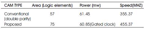
Table 1. Comparison using Gated Clock and Without Gated Clock Technique
In the comparison of conventional(single parity bit) and proposed CAM(double parity bit) and weightage (MSB& LSB), speed and area is increased using double parity bit more than bit single parity. Using weightage, the searching speed is increased and power is also increased as shown in Table 2.
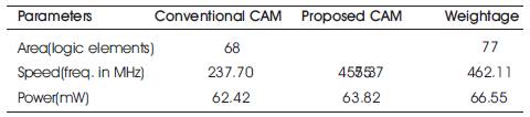
Table 2. Comparison for Conventional and Proposed Cam and Weightage
The conventional CAM circuits and parity bit based architectures, offer some advantages such as reduced sensing delay and increased frequency. By using the parity bit based CAM, the searching speed is increased and the delay is reduced. At the circuit level, two basic CMOS cells are used, namely the NOR cell and the NAND cell. The combination of the cells in a match line structure is represented as a CAM word. The proposed methods are double parity bit and double parity bit with weightage. Using of these methods, speed, area and power are increased when compared to single parity bit. By using gated clock technique, power consumption is reduced with increasing speed and area. The main CAM challenge is to reduce power consumption associated with the large amount of parallel active circuitry, without sacrificing speed.